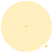
In the past i have created coils and imported then in fritzing and with some hassle it usually worked. But in the latest version of fritzing it has become more difficult. to create such ‘pcb parts’.
It would be nice if .SVG was allowed to be uploaded here on the forum.
Ultimately it would be ideal if this would become a standard part in fritzing with the option to configure number of turns inner diameter outer diameter, and trace width. But for now it would be nice to just have a part that can be imported without too much trouble so that i can build a few custom coils in Inkscape.
My part has
a id=silkscreen layer (not visible in the png but it is there)
a id=copper0 layer
Link to file. (I saved this as plain SVG in inkscape)
Please don’t forget to tell us what is all wrong with it .
I have a few other ideas like this.
I’ll also upload the inkscape SVG. (thats still on another PC somewhere…)
Edit =============
Turns out that the post img website converted the.svg to .PNG sigh
Pastebin gives captcha errors… pffffffffffffffff Any hits for a better way of sharing .svg online?
If possible without the need of creating more accounts (that generate spam)?
Google is not helping much either. Every site i’ve tried so far all reject .svg or convert it to png.
What program did you use to edit the file? When i open it in inkscape it works fine but when i try to modify it then inkscape gets confused for some reason. The spiral turns black with a very wide tracewitdh and it no longer can be edited.
I’m trying to make a few variations. Different trace width, Inner diameter, outer diameter, different number of turns, induction value, specific ‘wire’ lenght for easy frequency prediction etc.
Ideally it would be nice to have a part widget that gives the option to set these parameters and connect the start and end of the coil to a pad.
I took your coil and edited it in CorelDraw. Inkscape .svg and CorelDraw .svg are not compatible; Inkscape .svg will disintegrate when I imported it, but I managed to salvage the coil and clean up the code. I use CorelDraw because I use it in my business and that is what I am familiar with.
You can use Inkscape and do everything you want, if you open it up Pancace_Coil_1 in Notepad++ and look at the structure of the code then you can duplicate it in Inkscape. To start with, your layers were not named correctly; your layers and pins were all named with dash (-) numbers, i.e. copper0-4, copper1-9, connector0pin-9, etc. This all needs to be relabeled in your in your XML editor. When saving, make sure you save it a Plain SVG and not Inscape SVG.
Make sure you are looking at my updated copy… the Pancace_Coil_1 that is on Fritzing now. Coil-0 and Coil-1 should be only in the top layer (copper1), connector0pin and connector1pin needs to be on both layers (copper1 and copper0). copper0 and copper1 are imbedded layers… see as follows;
connector0pin and connector1pin in the .svg need to be identical in the .fzp, pcbView, layers. coil-0 and coil-1 are just names, they can be anything you want, but not in the fzp.
Not that I know of, when saving in the parts editor, it updates the part in Fritzing.
btw, since the coil in on a copper layer, I don’t think it will be covered by the solder mask. I think it would need to be a trace for the solder mask to cover it. I don’t know if that is possible or not.
The coils are for random experiments. Wire wound coils are cheaper, but have different properties and pancakes are a lot of work to do with wire especially when you want a bigger space between the windings.
Then there is RFID. a coil with a large inner diameter where you can place the coil around the electronics.
Qi style stuff? as QI receiver coils perhaps to charge low power wireless sensors.
But first things first… an easy to use coil.
I’m home way too late… i’ll better get some sleep first and try more tomorrow with a fresh mind and the help file open.
Here is your pan-coil done-up inside of Inkscape. Just a little FYI for anyone interested in the inkscape process of making partspan-coil-test.fzz (53.2 KB)
This gives me a lot new insights that I couldn’t peice together from the wiki
What still confuses me is the file formats, and what goes where. Eventhough there is this wikipage that explains it all.
I think it would be nice to have some graphical content in there as a picture can often tell more. Just by showing it. So I’m very pleased with the files!
I’m now going to try and tit it all together, it looks like I need a bit more time then I expected.
I’ll first make all the initial graphics i have in mind, then do all the xml stuff (i think i need some help there to make it right) then the file structures and and file containers. And whatever else that needs to be done.
So guys, Thanks thanks thanks for pointing me in the right direction.
Still I need to figure out how I did this in an older version of ftitzing, that worked fine for making stuff like this in a more quick and rough way. I made a image in frizing and loaded it in one of the widgets and that just did the trick back then. Or at least it did for DIY etching…
BTW who could I ask if it is possible to launch the Parts editor on its own without launching the fritzing app itself. (If that is possible)
Because I often do this stuff on a tiny netbook I drag along with me.
There is currently no way to run the parts editor outside of fritzing that I know of. Unless I am missing something, the part’s-editor files are directly compiled as part of the main fritzing application. This could be a possible future feature request.
I found a way, when I open the parts editor then fritzing itself can be closed. The parts editor stays open.
Just what i need. Though i hope nothing gets messed up this way. Now i can Shift+tab between Inkscape and Parts editor without having to choose between 2 fritzing logo’s maybe a yellow logo for parts editor would make sense.
Anyhow, now i’m searching for the design rules file (.DRU?) I want to know the absoute minumum etchable tracewidth and minumum space between traces so I can optimise my coil to that. Maybe with a little extra margin
My goal is to make a long as possible pancake trace on a 5 cm round board… (to find the lowest possible resonance frequency for a coil on that space) The longer the trace the lower fRes. and i can calculate an estimated impedence value for it (and afterwards measure how far my calculations are off )
The DRC has the options homebrew, professional and custom, but i cant find the actual values of homebrew and pro.
What would be best in the schematic view? Just keep the normal solenoid symbol? Personally I would like to draw a pancake for the schematic view aswel just to avoid confusion about the inside and outside pin.
Could this be acceptable coil symbol as a schematic part?
For me this would be ideal, although it is not a standard symbol for a coil. But if you use both a solenoid and a pancake in the same project then I is clear at one glance who is who and more important what is connected to the inner winding and what to the outer winding.
And if someone can scrutinise the xml that would be nice too.
Silkscreens can be top and bottom; In your core parts, PCB view, you can insert text or image on either side of the board. You can draw any image you would like in Inkscape, save it as .svg, and insert on to the board.
EDIT: silkscreen0 seems to be the bottom silkscreen layer
Is there a spec file that covers all the files, and all their respective layers and other name tags?
i see
connectorX
connectorXpin
connectorXpad
connectorXterminal
connectorXleg
when do i use who The wiki doesn’t seem to cover them all (just like it does not seem to mention a second silkscreen layer by name)
How to use metric and imperial mixed in one file. (without going insane)
I noticed that Frizing Inkscape Illustrator (and also Corel) all seem to do things a little bit different. And are not 100% compatible with eachother.
This specially comes to light when you change a Imperial to a Metric value.
Then the trace width always gets messed up.
The thing is this, I calculate and draw my coils in metric, since I don’t know how to do this in imperial.
Though Fritzing seems to prefer Imperial. Is that correct? I see more and more EE stuf moving to Metric (1mm and 2mm pitch headers for instance)
So what will the future require? Metric seems to be more universal.
Since all of this is still beta i’m not expecting it to be complete, though i find it difficult to get my head around all of the details when i can’t seem to find the actual info about the detail that i try to figure out.
So if this info is listed somewhere that would be a great help.
A table or a cheat sheet style 1 page document that covers all the tags is what i have in mind. If really non exists then i’ll give it a try to start one.
i have a weird ratsnest line showing up that i cant figure out where it comes from.
the breadboard view is a bit weird, how can that be done better?
the pcb view has a large squre around the center pin that was smaller when i designed it.
any idea why this happened?


 Though i hope nothing gets messed up this way. Now i can Shift+tab between Inkscape and Parts editor without having to choose between 2 fritzing logo’s maybe a yellow logo for parts editor would make sense.
 )
)
