Hmm, maybe the part I was modifying had the same problems? I am not very familiar yet with designing a part from scratch, nor all the rules it must check.
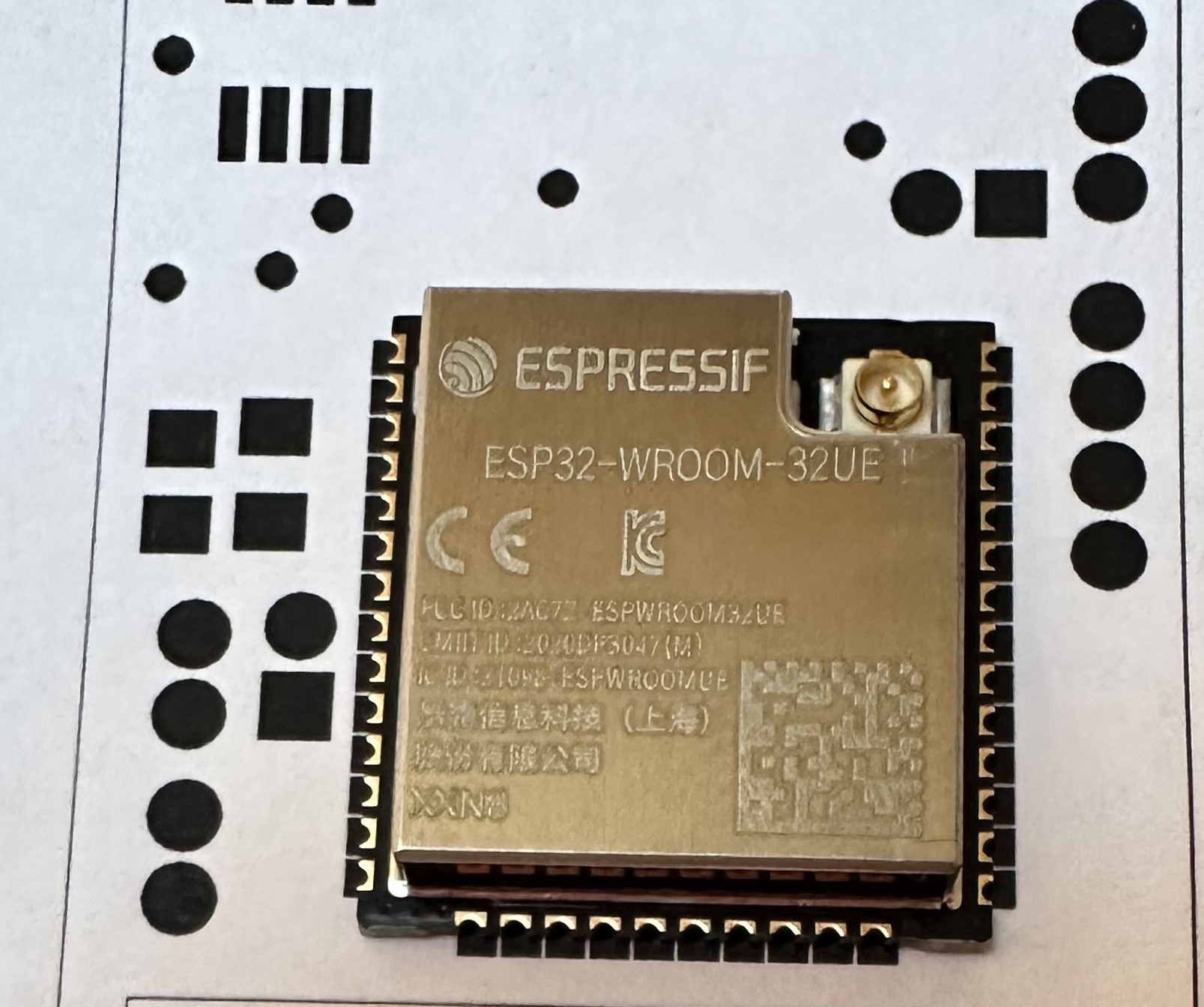
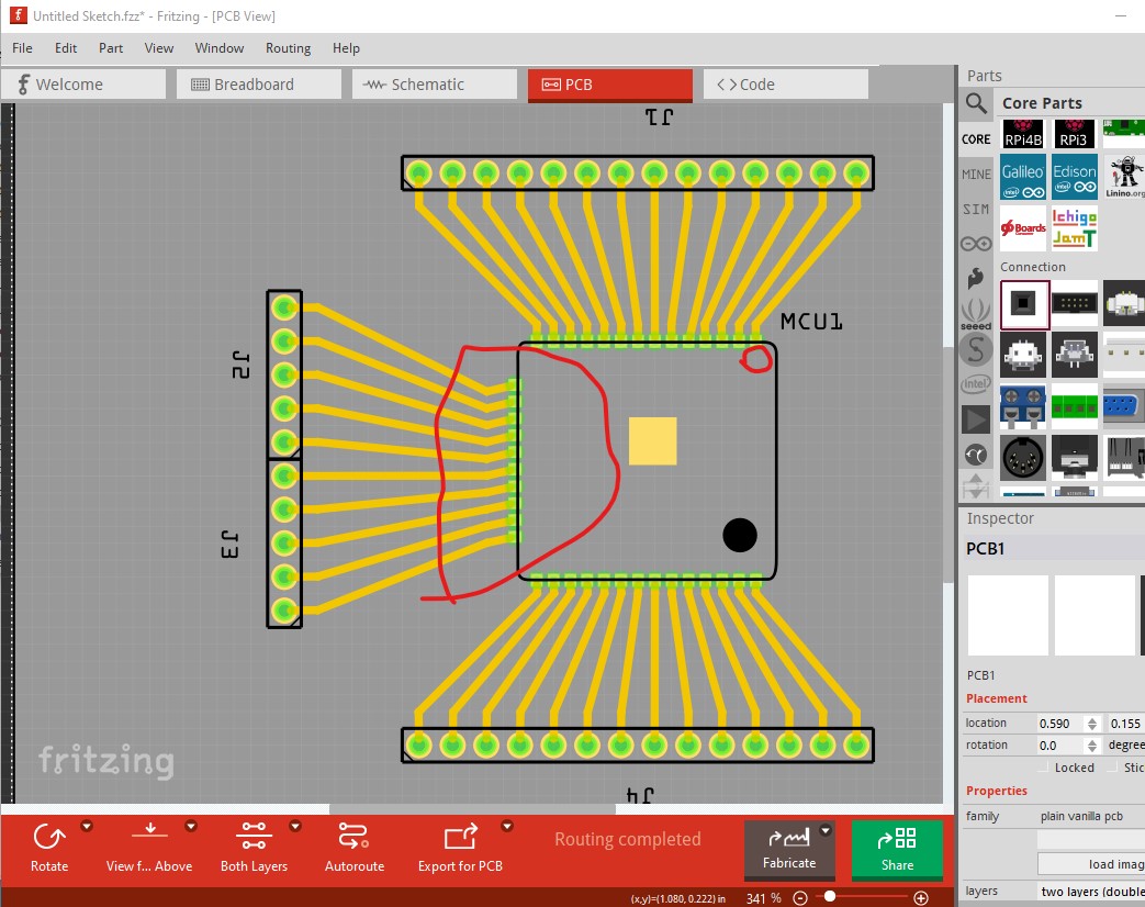
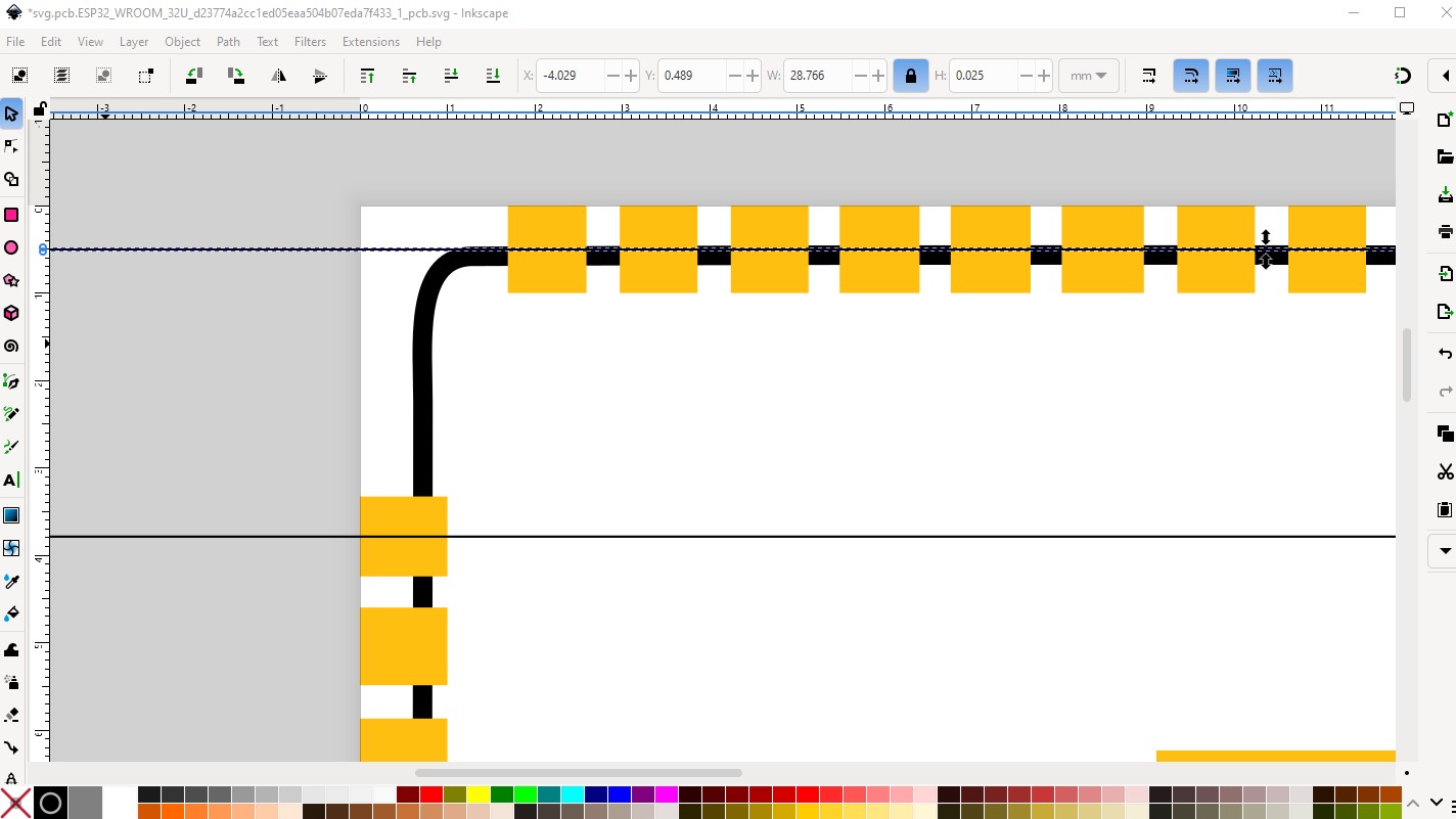
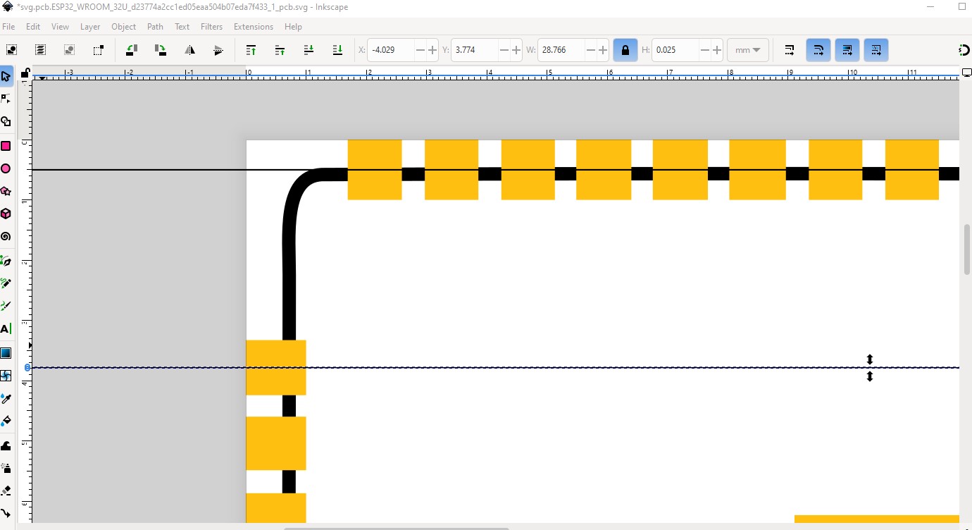
I created a test PCB and printed it to check the alignment to the real chipset.
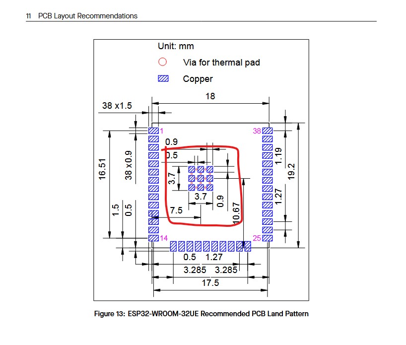
Over all looks fine, a few issues though (mostly in pcb.) You are missing a ground connection to the thermal pad on the bottom. There is a pad there but it has no connection (and shouldn’t be a pad.)
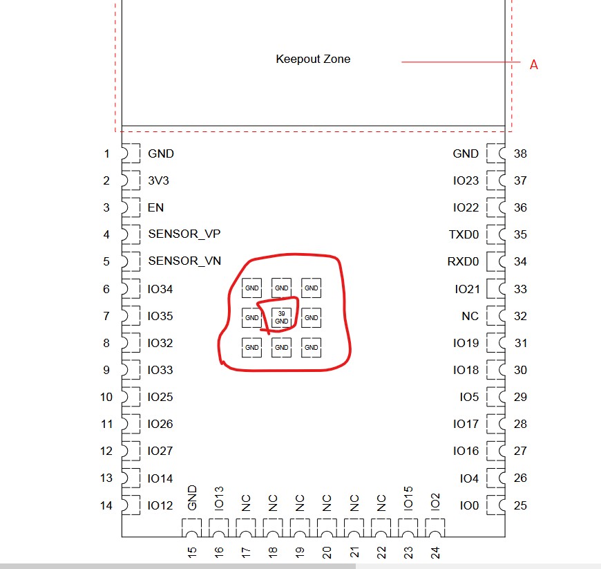
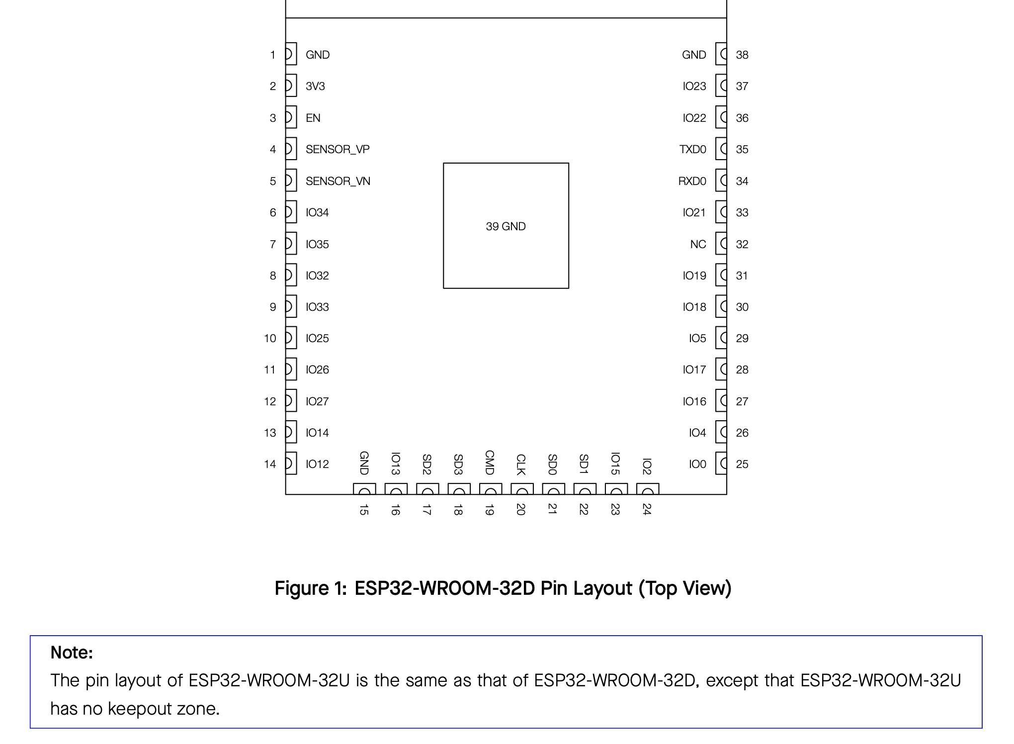
The thermal pad is intended to be squares (the large pad may be fine as well I don’t know but they are recommending pads, and I would follow their recommendation.) They also indicate vias (which Fritzing can’t do in a SMD part) to a presumed but not specified thermal pad on the other side of the board.. Both of those can be added in the sketch (drag in a pad on the bottom of the board and vias where needed, put them in silkscreen to place them.) The pads are pin 39 and need to be ground
and should appear in schematic. That done, pcb looks suspicious. I would expect the end pads to be on a 0.05in grid and they are not which may mean the bottom pads are misaligned
It would be a good bet to check the pcb svg to make sure the pin alignment matches the datasheet I expect. As noted I think they should be on a 0.05in grid and they are not. here. I didn’t check all the measurements to verify that but it appears the bottom pads should be centered between the end pads and thus should likely align to the 0.05in grid. As @RAPTOR7762 noted it is preferred to have an adapter plate in breadboard, but either way will technically work.
Thank you. I’ll double check the print. I did not change the pads alignment from the part I modified. Just the top part, where the antenna is located for the wifi version.
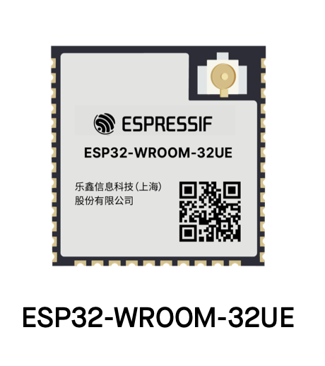
And yes, the internal GND pad was just graphic. I don’t intend to use it. And strange enough there is also a 32U part (ESP32 WROOM 32U) that has a whole pad there, not 9 smaller pads. Somehow I ordered both types. Since there are already 3 or 4 grounds on the side pins, I don’t need that internal pad.
I would check that the pad is connected to the other ground pins. It may or may not be. With RF grounding is critically important so you may find it the pad isn’t grounded the part doesn’t work correctly. The internal pads are often also intended for heat dissipation (and I would guess that is the case here, as the vias are likely to promote heat dissipation on the other side of the board although that isn’t specified anywhere I have seen and is thus just speculation.)
I was afraid of it being a heat dissipation pad. But then I found in the old specs that is was not required to solder that pad.
Page 33: Soldering Pad 39 to the ground of the base board is not a must. If you choose to solder it, please apply the correct amount of soldering paste. Too much soldering paste may increase the gap between the module and the baseboard. As a result, the adhesion between other pins and the baseboard may be poor.
OK. It appears that pcb is likely correct too. While the pads are shorter than the recommended 1.5mm at 1mm, the spacing between the center of the horizontal pin and the center of the vertical pin is the required 3.285mm
so the offset from the grid appears to be intended (if odd!) so your part is likely fine. You would likely need to change the grid size to center the end pins when routing traces there which will be a pain in the ass, but apparently intended (I don’t see a reason why though.)