Unless this was an incorrect file, you are going backwards. There is still no breadboard layerId, and schematic is broken in a way I don’t understand. The x alignment is offset by 0.05in and I don’t know why (and can’t correct it in any way I have tried so far.)
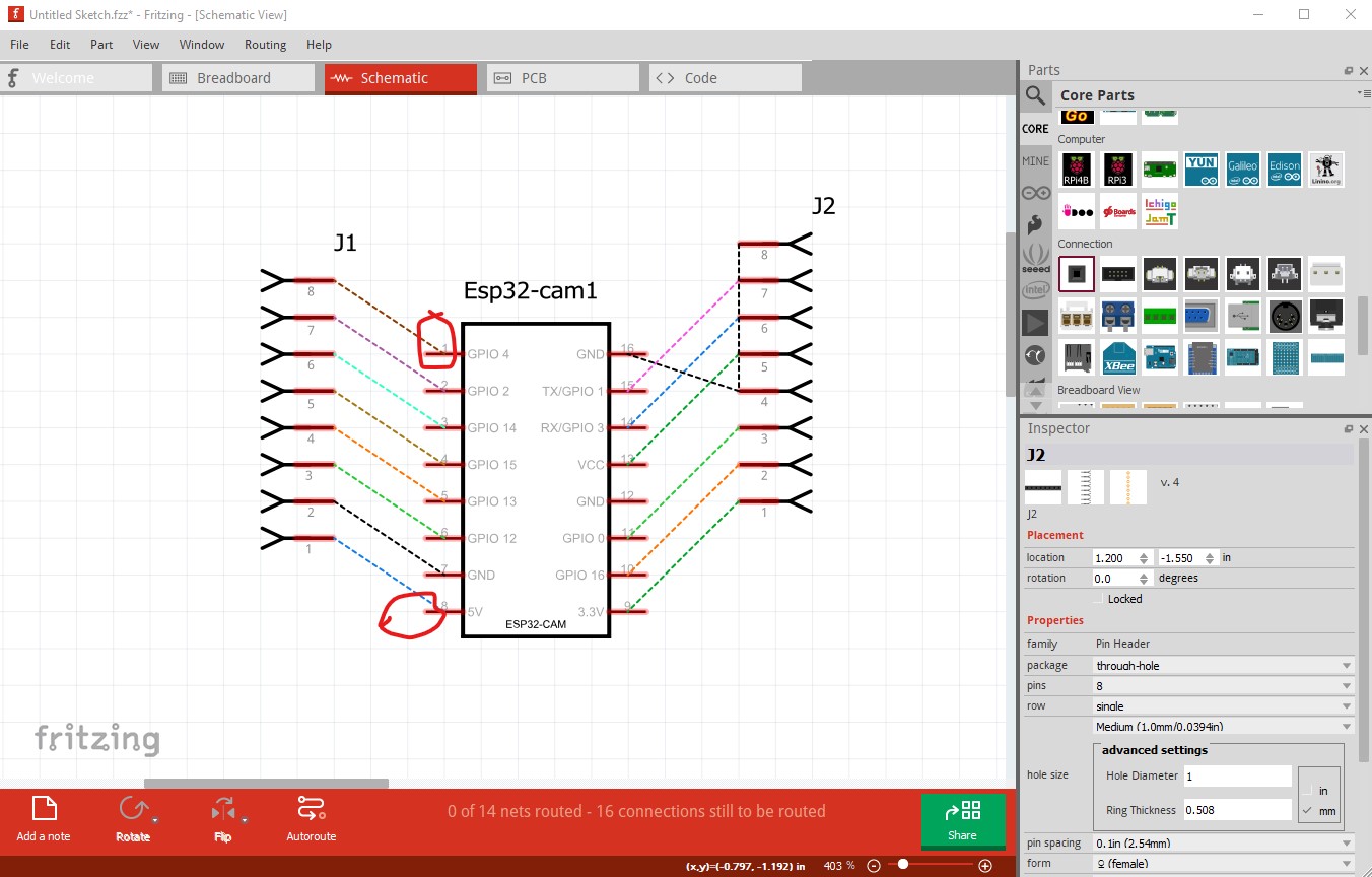
The end of the pin here should be on the .1 grid line, but it is offset by 0.05in for some reason. The svg looks correct to me but the problem persists. The terminalIds are all missing in the svg causing the connection in the middle of the pin.
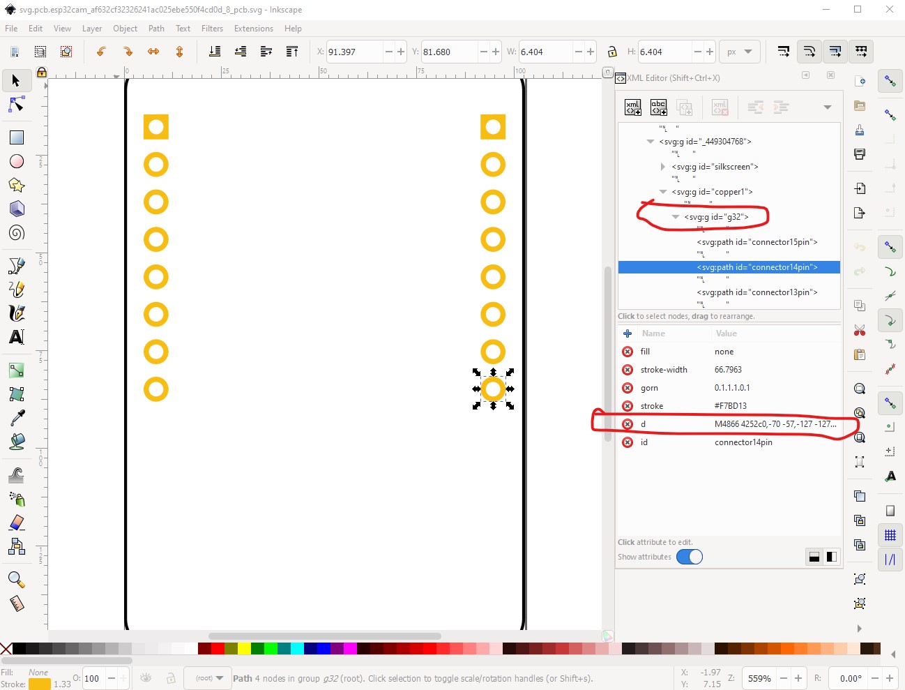
In the pcb svg copper0 is missing, so the pads are not correctly defined as through hole and the pads are all paths so the gerber code won’t drill holes for any of them. I’ll continue poking at the schematic svg to see if I can figure out why the offset.
edit: Found the problem in the schematic svg. It is missing these two parameters in the first lines
x=“0in”
y=“0in”
the original is
<?xml version='1.0' encoding='UTF-8' standalone='no'?>
 <svg
   xmlns:dc="http://purl.org/dc/elements/1.1/"
   xmlns:cc="http://creativecommons.org/ns#"
   xmlns:rdf="http://www.w3.org/1999/02/22-rdf-syntax-ns#"
   xmlns:svg="http://www.w3.org/2000/svg"
   xmlns="http://www.w3.org/2000/svg"
   viewBox="0 0 3387.3635 5040.1533"
   xml:space="preserve"
   height="0.90000004in"
   width="0.60475165in"
   version="1.1"
   id="svg294">
   <metadata
and it needs to be
<?xml version='1.0' encoding='UTF-8' standalone='no'?>
 <svg
   xmlns:dc="http://purl.org/dc/elements/1.1/"
   xmlns:cc="http://creativecommons.org/ns#"
   xmlns:rdf="http://www.w3.org/1999/02/22-rdf-syntax-ns#"
   xmlns:svg="http://www.w3.org/2000/svg"
   xmlns="http://www.w3.org/2000/svg"
   viewBox="0 0 3387.3635 5040.1533"
   xml:space="preserve"
   height="0.90000004in"
   width="0.60475165in"
   x="0in"
   y="0in"
   version="1.1"
   id="svg294">
   <metadata
to remove the 0.05in x offset (although I don’t know why.)
Peter