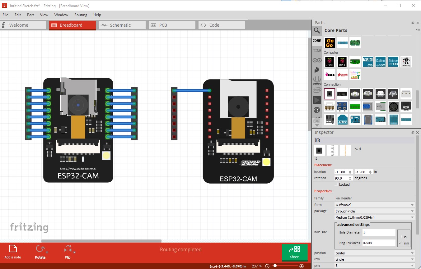
Esp-32 cam board
ESP32-Cam.fzpz (21.4 KB)
1 Like
I ran the contents of that part file through FritzingCheckPart. Here is a summary of what it reported, and what I noticed doing a manual inspection and smoke test in Fritzing.
The copper0 and copper1 layers (groups) in the pcb svg should be reversed. copper0 should be ‘inside’ copper1, instead of the other way around.
The “breadboard” layerId specified in the fzp part definition does not exist in the matching svg image. This will “appear” to work in Fritzing, but exporting a sketch to an svg image will not include the part. The first/outer wrapper group element should be changed tThose should be put intributes for connectors in the schematic view, which do not actually exist in schematic svg. These should exist in the svg. They are used to give Fritzing a reference point, to “snap” wires to. Without this, wires attached to the connectors will be drawn to the middle of the connector pin line, instead of to the end.
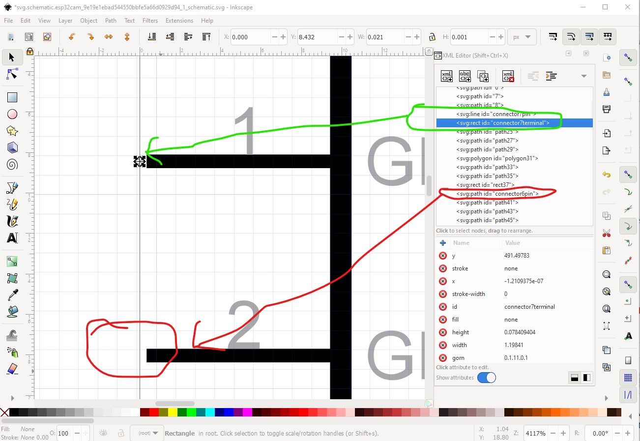
The connnector«n»terminal elements should be circles, rectangles, or lines centered at the end point of the corresponding connnector«n»pin elements that wires should connect to. Usually with fill and stroke = “none”, so they are not visible.
In the pcb svg, connector0pad and connector8pad have been created as “rect” elements. That does not have a radius, so exporting to gerber will not create drill holes for those connectors. The way to create square (or other non-circular THT pads) is to use a circle element for the the connector«n»pad elements, then add additional (usually path) elements to expand the circle. Do not cover the hole in the circle with the extra graphics, but do overlap with the ring (stroke) of the circle as much as possible, so that Fritzing will detect the extra graphics as being part of the pad. The extra graphic elements do not have a pad id.
This board has 3 GND pins. A ‘bus’ entry should be created for those, so that Fritzing knows that anything wired to one of those pins is electrically connected to the other GND pins as well.
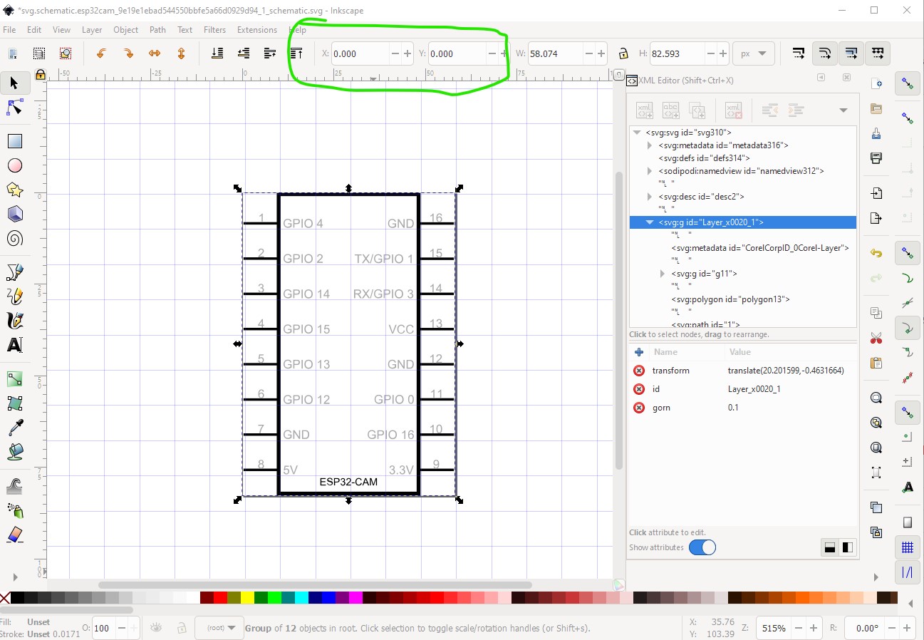
The schematic svg should be scaled so that the connector pins on each side are (exactly) 0.1 inch apart, and 0.1 inch long (sometime 0.2 inch long). The 2 rows of pins should be a multiple of 0.1 inch apart. Specifically, the connector«n»terminal elements should all be exact multiple of 0.1 inch in both x and y directions from every other connector«n»terminal element. This lets the part position cleanly in relation to other parts, and connection wires will line up nicely.
With the family for the part defined as “esp32”, the variant should be something else. “variant 1” is too likely to conflict with some other part in the same family. “esp32 camera” could work, although that is still likely to not be unique for other esp32 “sibling” boards. The combination of property names and values needs to be unique for every loaded Fritzing part. Otherwise Fritzing has now way to pick the correct one to use. Or actually, the user has no way to tell Fritzing which one to use. Internally Fritzing uses the moduleId value, which also has to be unique.
If there is a web page for this part, the fzp metadata should include a <url> entry pointing to it. This should be a place to find out more information, even if that is just a page to order the part. Data sheet type web pages are another option.
The “important” ones from that, the ones that will cause using the part to “break” during use (export), are the missing layers and no circle for the pcb pads. The rest are more cosmetic or limiting. The part will work, but the sketch might not be as clean as it could be, or the part can not be loaded at the same time as some other esp32 family parts.
In addition to @microMerlin 's comments, my first advise is be lazy. Someone else asked for this part a year or so ago and found one (which is broken) that I fixed. It is available here:
a google search of the form “fritzing part esp-32 cam board” will find it. The fixed part is the left hand part in the following images.
breadboard, pretty much identical
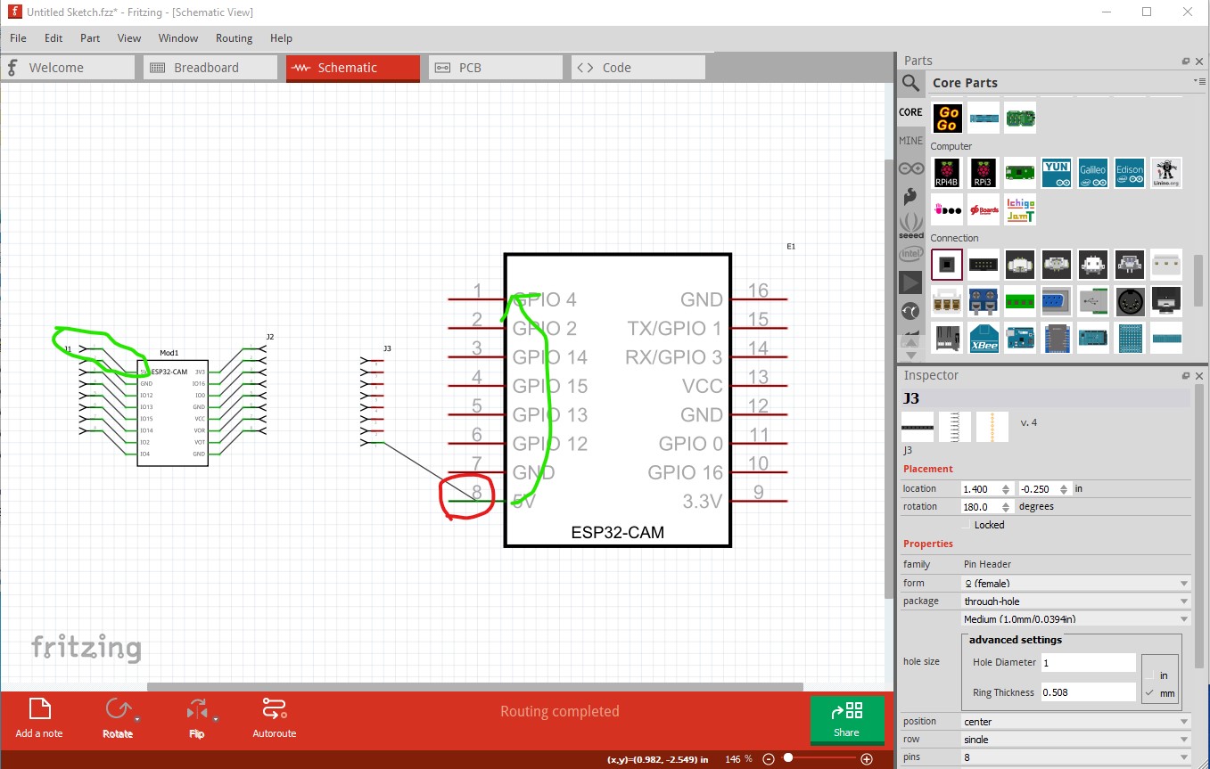
schematic
some problems as noted the lack of terminalId in schematic connects in the center of the pin. The schematic is too large (schematic space is valuable!) and the pins are inverted from breadboard (which isn’t an error necessarily as they connect correctly, but is confusing.)
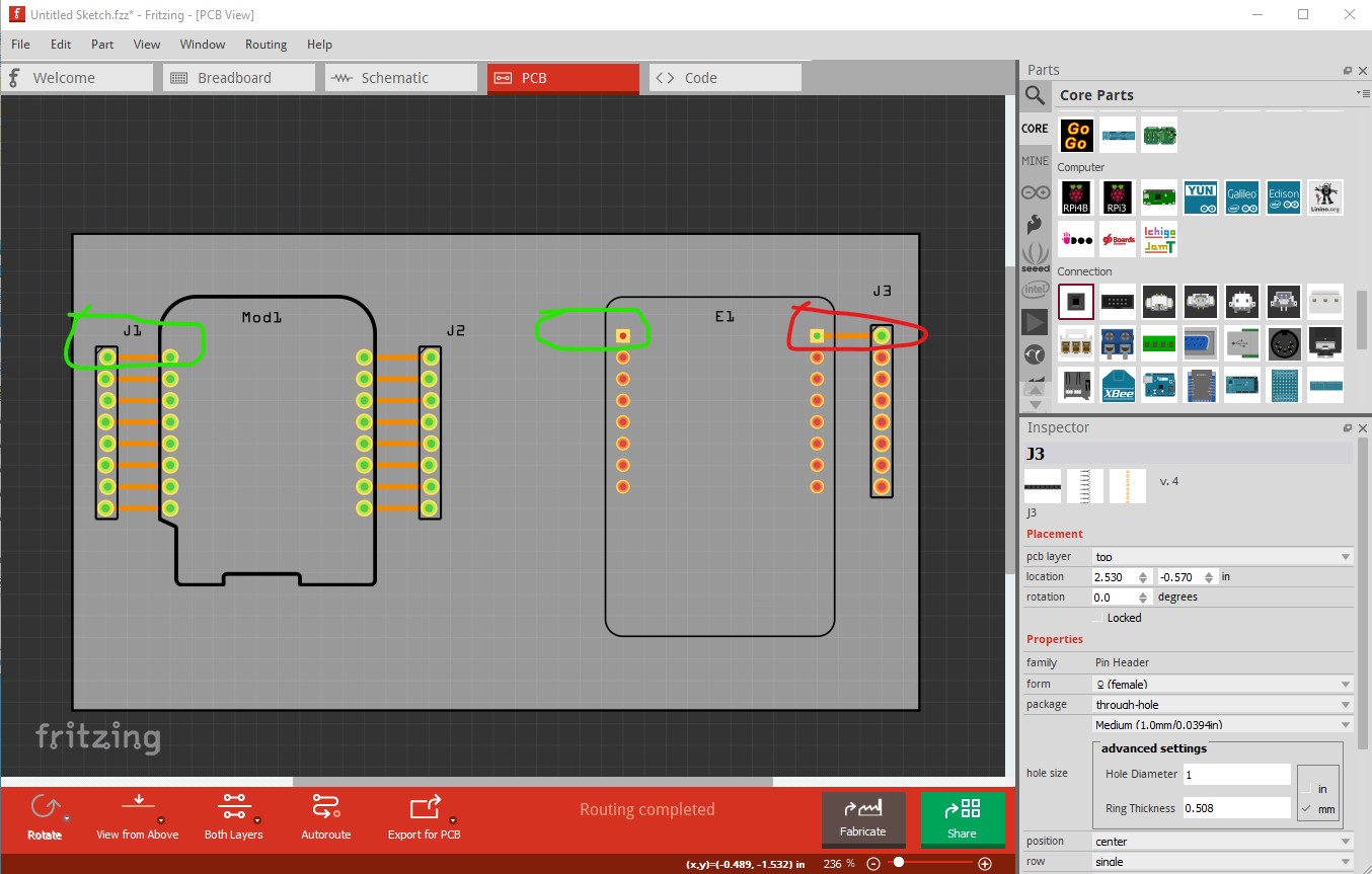
pcb has the main problem, the alignment is incorrect. It should be the same as breadboard but is inverted (you would need to mount the camera on the bottom of the board for the pins to maybe be correct!) The pin circled in red should be on the other side of the board (circled in green.)
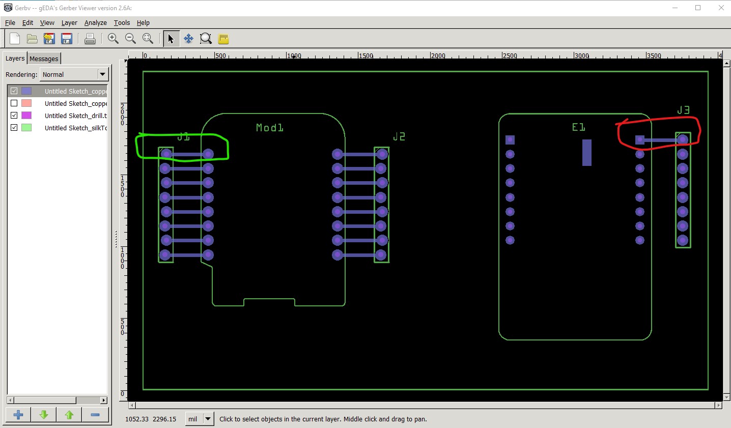
In the gerber output the same thing applies the pin should be on the other side of the board.
Despite what FritzingCheckPart reported all the drill holes are present (although they appear to be too small for 0.1in pins
Peter
Thank you for your comments I’ve fixed the mistakes.
ESP32-Cam.fzpz (18.3 KB)
This version is not fixed. Still no breadboard layer, no schematic layer, no terminalId elements, no url, still not very unique or descriptive property information.
FritzingCheckPart still complains about no radius for the 2 connector pads, but Peter says gerber export is working anyway. Or “maybe” working, since the holes seemed smaller than expected. The holes are “probably” being created by the 2 circle elements that do not have a connector id.
Here is a more specific list of problems and fixes.
Error 69: File
‘svg.breadboard.esp32cam_9e19e1ebad544550bbfe5a66d0929d94_1_breadboard.svg.bak’
At line 10
Found a drawing element before a layerId (or no layerId)
to fix this the easiest way is to change this
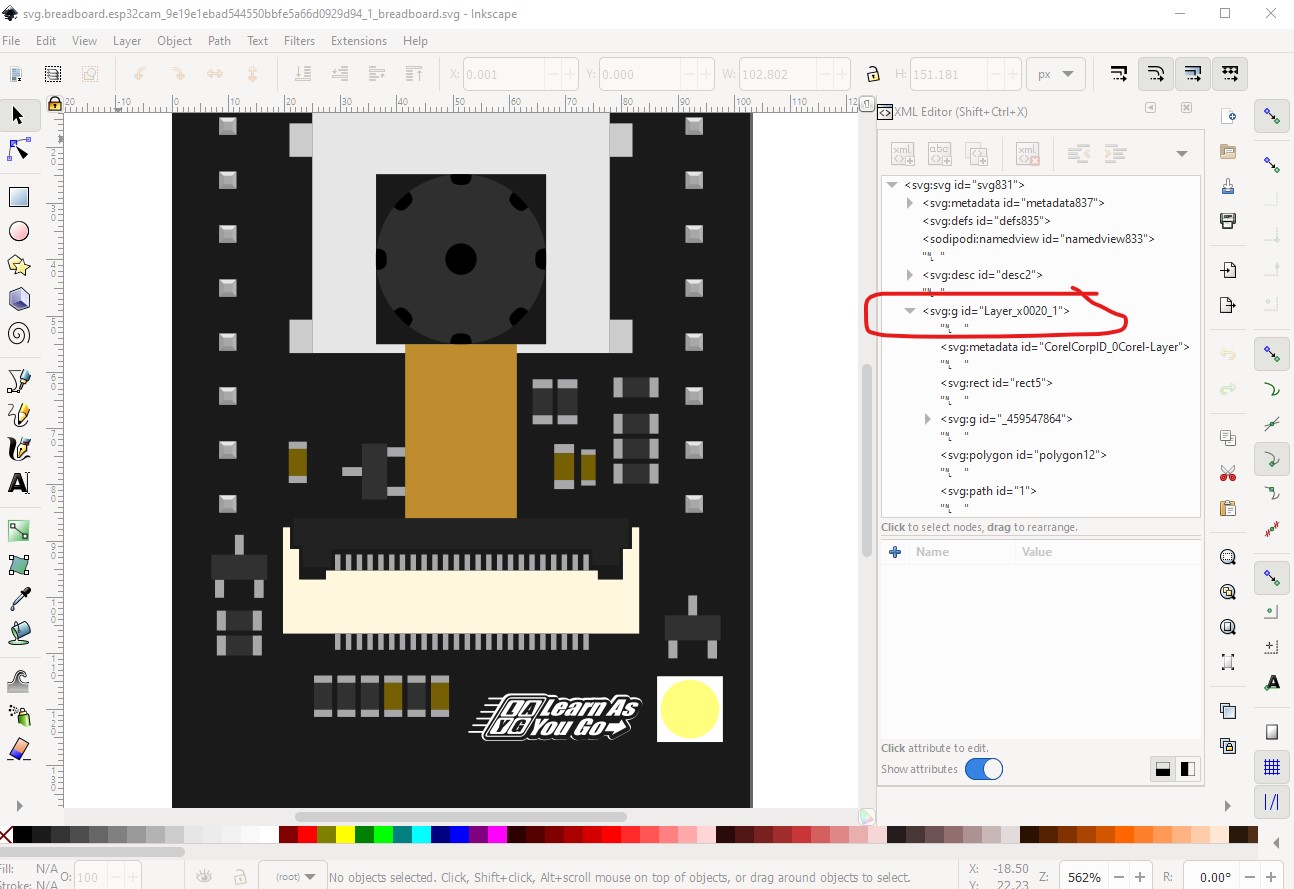
to this:
to match the layerId set in the .fzp file here:
<breadboardView>
  <layers image="breadboard/esp32cam_9e19e1ebad544550bbfe5a66d0929d94_1_breadboard.svg">
    <layer layerId="breadboard"/>
  </layers>
</breadboardView>
Same for schematic
Error 69: File
‘svg.schematic.esp32cam_9e19e1ebad544550bbfe5a66d0929d94_1_schematic.svg.bak’
At line 11
Found a drawing element before a layerId (or no layerId)
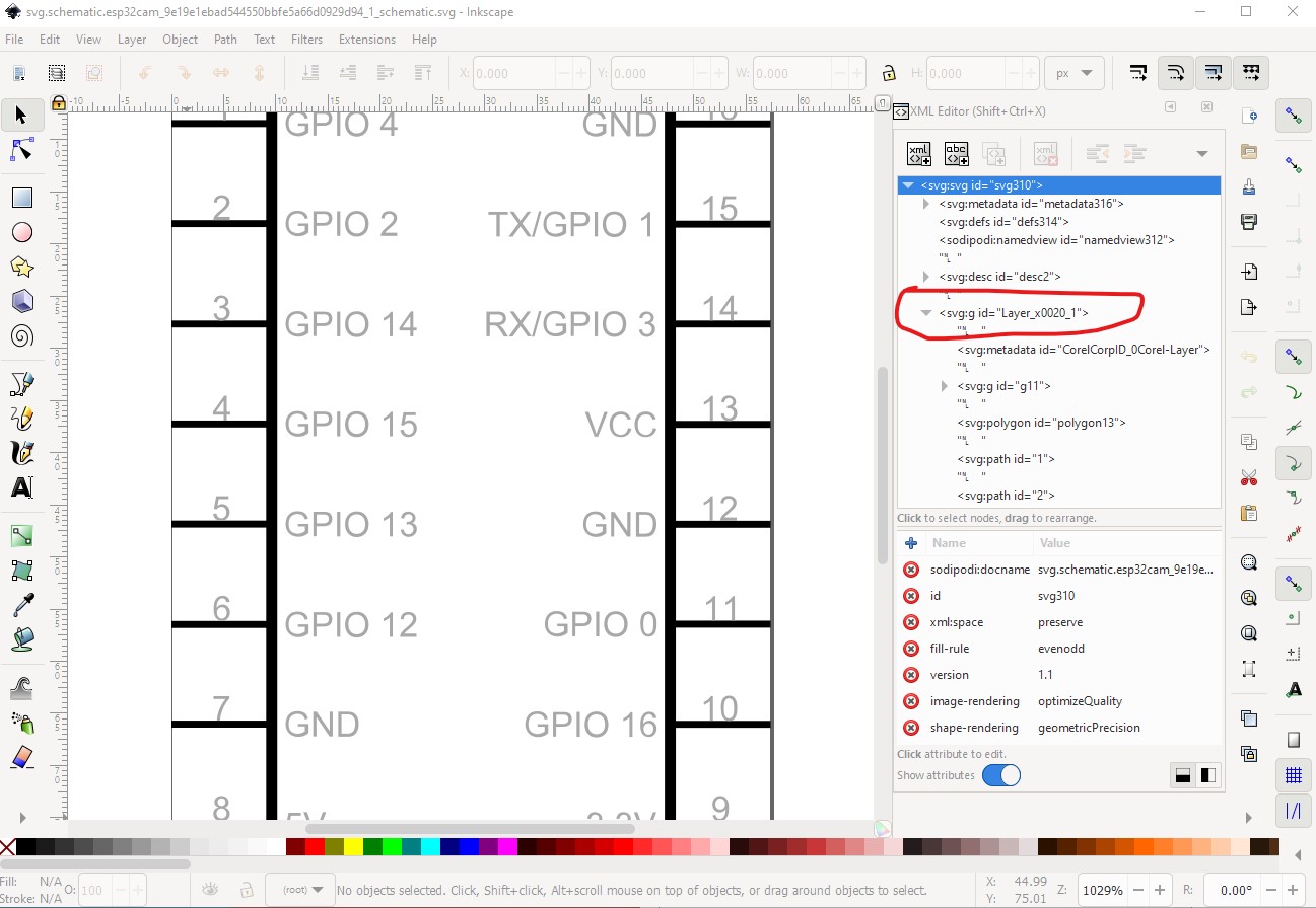
changing this id to schematic will fix the layerId problem
<schematicView>
  <layers image="schematic/esp32cam_9e19e1ebad544550bbfe5a66d0929d94_1_schematic.svg">
    <layer layerId="schematic"/>
  </layers>
</schematicView>
It needs to match spelling and case with the layerId in the fzp file. There is another problem that FritzingCheckPart won’t catch in that the schematic is not aligned to the grid and several pins lack terminalIds causing the wire to connect to the middle of the pin. The misalignment is caused by the image not starting at 0 0 as Fritzing expects.

In Inkscape I would do edit->Select all then Edit->Resize page to selection to correct that like this:
I don’t know how to do that in Corel Draw though. The terminalId problems are here from FritzingCheckPart
Error 18: File
‘part.esp32cam_c101243d9ce29005d425b252d8f49fb5_2.fzp.bak’
Connector connector5terminal is in the fzp file but not the svg file. (typo?)
svg svg.schematic.esp32cam_9e19e1ebad544550bbfe5a66d0929d94_1_schematic.svg.bak
Error 18: File
‘part.esp32cam_c101243d9ce29005d425b252d8f49fb5_2.fzp.bak’
Connector connector6terminal is in the fzp file but not the svg file. (typo?)
svg svg.schematic.esp32cam_9e19e1ebad544550bbfe5a66d0929d94_1_schematic.svg.bak
Error 18: File
‘part.esp32cam_c101243d9ce29005d425b252d8f49fb5_2.fzp.bak’
Connector connector14terminal is in the fzp file but not the svg file. (typo?)
svg svg.schematic.esp32cam_9e19e1ebad544550bbfe5a66d0929d94_1_schematic.svg.bak
Error 18: File
‘part.esp32cam_c101243d9ce29005d425b252d8f49fb5_2.fzp.bak’
Connector connector0terminal is in the fzp file but not the svg file. (typo?)
svg svg.schematic.esp32cam_9e19e1ebad544550bbfe5a66d0929d94_1_schematic.svg.bak
That is because the associated terminalId isn’t in the svg. Here connector7 has both, but connector6 only has the pin no terminal.
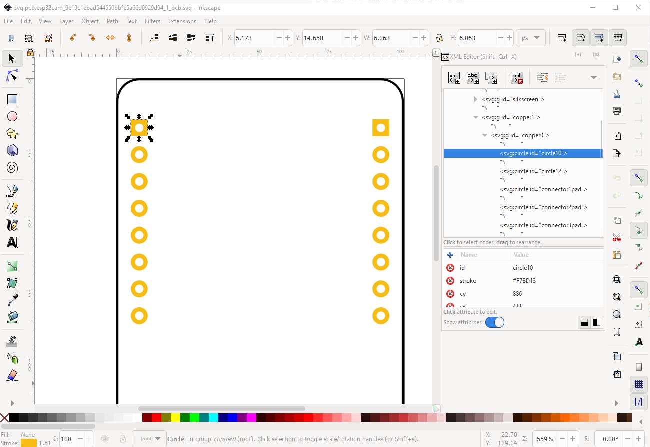
pcb is mostly good, the pins are in the correct place
Checkpart is unhappy because the pins are not on the circles associated with the pads
Error 74: File
‘svg.pcb.esp32cam_9e19e1ebad544550bbfe5a66d0929d94_1_pcb.svg.bak’
At line 33
Connector connector0pad has no radius no hole will be generated
Error 74: File
‘svg.pcb.esp32cam_9e19e1ebad544550bbfe5a66d0929d94_1_pcb.svg.bak’
At line 34
Connector connector8pad has no radius no hole will be generated
As well there is a likely unintended copper pad which is invisible (but appears in the gerber output as copper) that likely should be removed

The easy way to fix checkpart’s complaint is to move the pin label from the rectangle (where it is now) to the circle (which creates the hole.) Either will work in practice but FritzingCheckPart can’t associate the rectangle (which won’t generate a hole in the gerber) with the circle that overlays it.
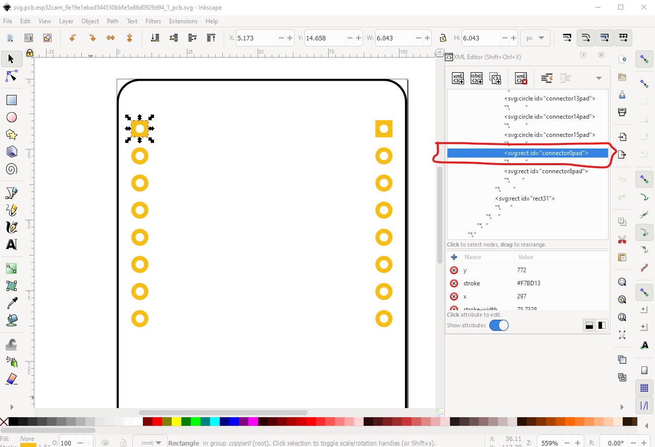
changing the connector0pad (which by the way should be connector0pin for a through hole although either will work) to the circle will stop this complaint.
exporting the pcb view as gerber and then editing the resulting drill.txt file indicates the holes are the wrong size. As we see from the header pins, the hole size should be 0.038in to take a .1 in header pin. Your pcb is using 0.031663in which is too small. I know how to correct this in Inkscape, but luckily the person that told me how to do this in Inkscape used Coral Draw and indicated what to do in Coral Draw in a forum post but at present I can’t find it. For Inkscape the calculation is
hole-size = pad-diameter - (2 * stroke-width) but Coral Draw is (or was in 2017 or so) different. I’ll continue searching and see if I can come up with the instructions. An alternative is to edit the pcb svg of a .1 header connector and copy / paste the pad from the header in to your svg. That should give you the correct pad size and hole size.
Peter
Its “Corel” not “Coral”. A search for “Corel” in the forum returns a reasonably short list to look through.
Thanks! That did the trick, here is the original post:
The Corel instructions aren’t as clear as they might be (and Steve no longer posts here) but they may be enough.
Peter
Thank you for the corrections.
ESP32-Cam.fzpz (18.8 KB)
The new version of the part in the above post is still broken.
There are no elements in the schematic svg file to match the terminalId references. As a result, wires in the schematic view attach to the middle of the connector pin lines instead of the end.
The fzp file shows both copper0 and copper1 for a through hole part, but the pcb view svg file only contains a copper1 layer. That creates an SMD part.
The pcb svg contains both connector«n»pin and connector«n»pad elements, but only pad is defined in the pcbView metadata.
Both the pcb pin and pad elements are now all path elements. There are no circles that would tell the gerber export to create drill holes.
The bus for the ground connectors looks good, although only the single “internal3” bus is needed. The empty internal1 and internal2 bus entries are not needed. The name does not really matter to fritzing, but changing “internal3” to “ground” (or something else more descriptive) makes the information easier to understand. Without needing to go look what connectors 1, 11, and 15 are.
It is still a good idea to add something else into the part properties to indicate that this is a camera module. I would add an extra property name, but changing “variant 3” to “camera variant «number»” would also do the job.
Still no url in the metadata. That is not required for a valid part, but helps people using the part in there own sketches.
Unless this was an incorrect file, you are going backwards. There is still no breadboard layerId, and schematic is broken in a way I don’t understand. The x alignment is offset by 0.05in and I don’t know why (and can’t correct it in any way I have tried so far.)
The end of the pin here should be on the .1 grid line, but it is offset by 0.05in for some reason. The svg looks correct to me but the problem persists. The terminalIds are all missing in the svg causing the connection in the middle of the pin.
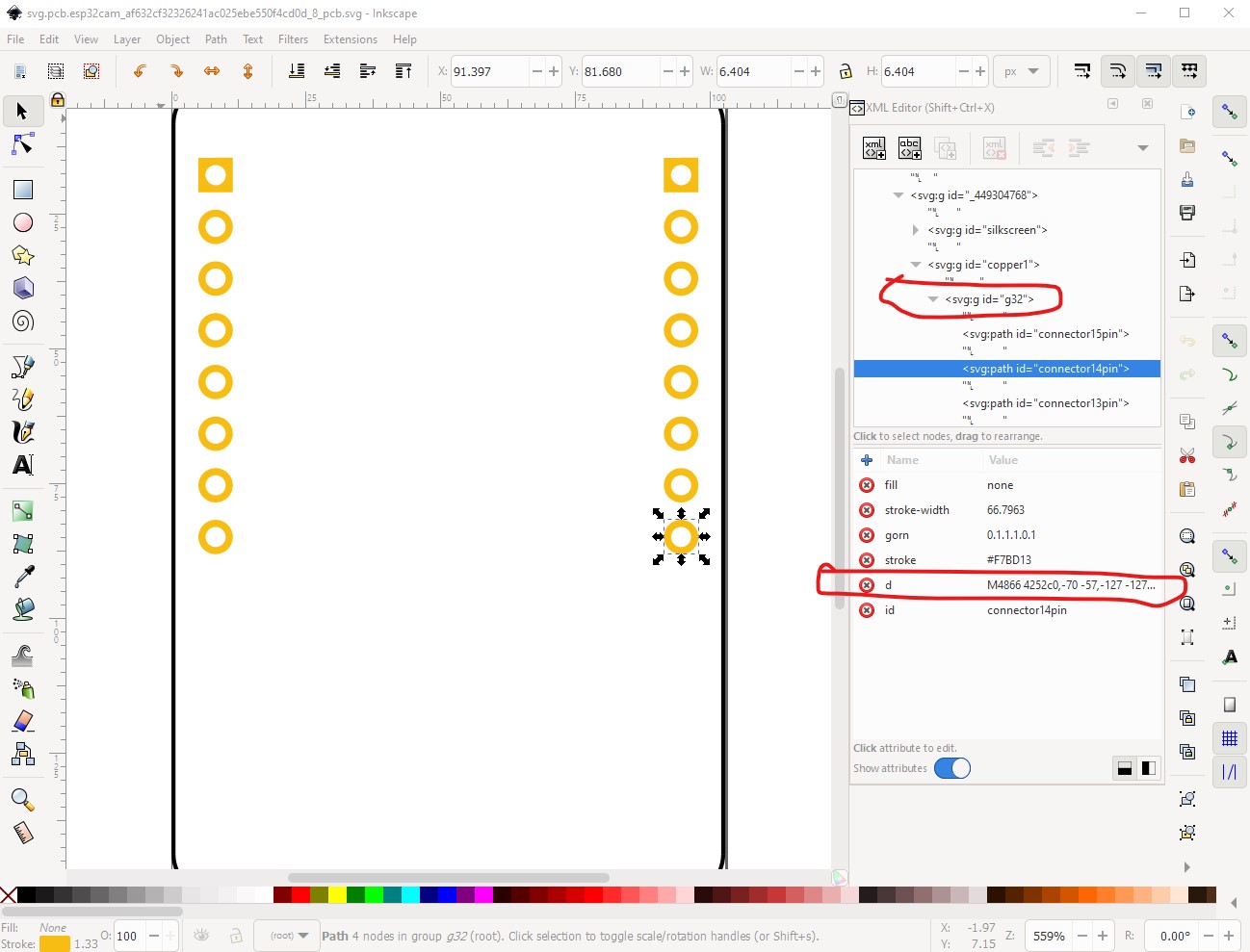
In the pcb svg copper0 is missing, so the pads are not correctly defined as through hole and the pads are all paths so the gerber code won’t drill holes for any of them. I’ll continue poking at the schematic svg to see if I can figure out why the offset.
edit: Found the problem in the schematic svg. It is missing these two parameters in the first lines
x=“0in”
y=“0in”
the original is
<?xml version='1.0' encoding='UTF-8' standalone='no'?>
 <svg
   xmlns:dc="http://purl.org/dc/elements/1.1/"
   xmlns:cc="http://creativecommons.org/ns#"
   xmlns:rdf="http://www.w3.org/1999/02/22-rdf-syntax-ns#"
   xmlns:svg="http://www.w3.org/2000/svg"
   xmlns="http://www.w3.org/2000/svg"
   viewBox="0 0 3387.3635 5040.1533"
   xml:space="preserve"
   height="0.90000004in"
   width="0.60475165in"
   version="1.1"
   id="svg294">
   <metadata
and it needs to be
<?xml version='1.0' encoding='UTF-8' standalone='no'?>
 <svg
   xmlns:dc="http://purl.org/dc/elements/1.1/"
   xmlns:cc="http://creativecommons.org/ns#"
   xmlns:rdf="http://www.w3.org/1999/02/22-rdf-syntax-ns#"
   xmlns:svg="http://www.w3.org/2000/svg"
   xmlns="http://www.w3.org/2000/svg"
   viewBox="0 0 3387.3635 5040.1533"
   xml:space="preserve"
   height="0.90000004in"
   width="0.60475165in"
   x="0in"
   y="0in"
   version="1.1"
   id="svg294">
   <metadata
to remove the 0.05in x offset (although I don’t know why.)
Peter
Thank you I believe the offset was caused when I designed it in CorelDraw it should be fixed.
ESP32-Cam.fzpz (18.5 KB)
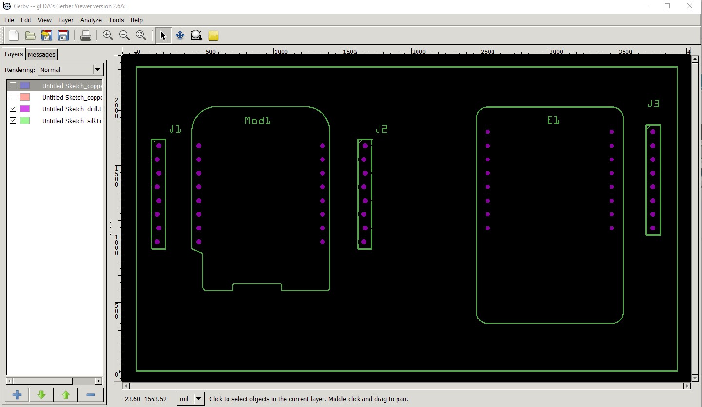
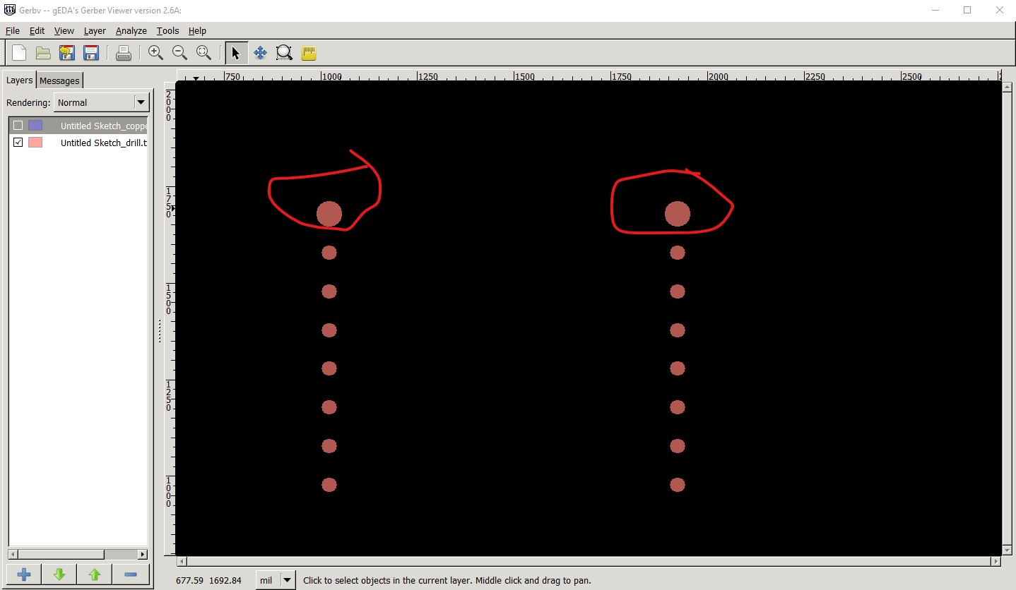
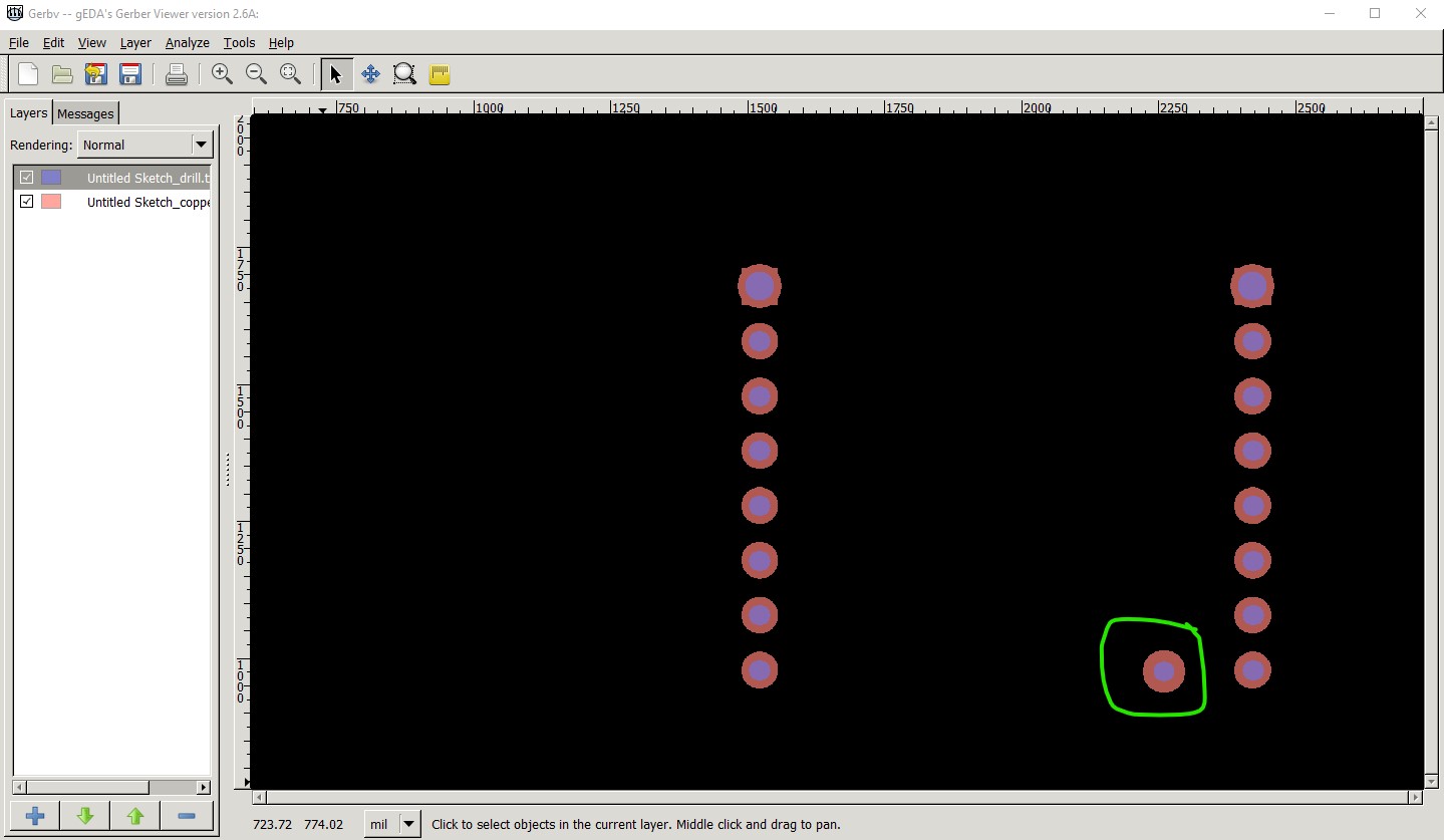
A lot closer, but still a couple of problems. FritzingCheckPart is still complaining about no holes, but that is a false positive. The holes are being drilled, they are just the wrong size. The two with the square pads are much too large and the others are a bit large. From the gerber drill.txt file
; NON-PLATED HOLES START AT T1
; THROUGH (PLATED) HOLES START AT T100
M48
INCH
T100C0.052858
T101C0.038926
T102C0.038000
%
The large holes (circled in red in the image below) are 0.052 in, the rest are 0.0389in (just a bit high) the bottom one is a proper pad I copied in at the desired 0.038in (it isn’t showing in this image!) The pads being paths makes changing the hole size difficult and thus it is preferred to use a circle for the pad where changing the hole size is easy to calculate (at least in Inkscape)
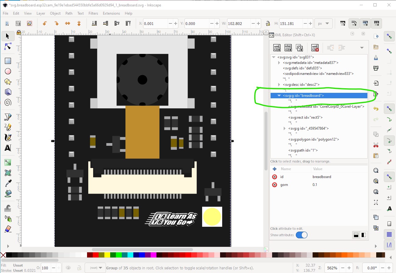
The breadboard svg is still missing the layerId:

changing this group to be breadboard will fix that like this:

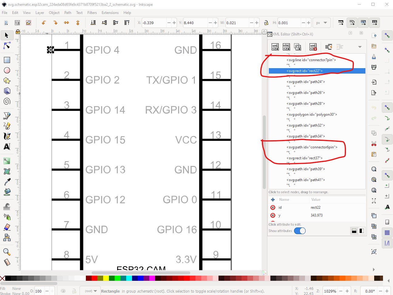
In schematic the terminalIds for connectors 6 and 7 are missing. The rectangles are there, they just are not named connector7terminal and connector6terminal so they don’t get used and the pin connects in the center of the pin.
finally here is the gerber output with a new pad defined as a circle and set to have a hole size of 0.038in
and the definition of the pad in the svg that creates this

In Inkscape changing the radius will change the hole size (without changing the x/y coords of the pad!)
Peter