Until I get a corrected part you will get the DRC error, it is internal to the YL-83 Rain sensor controller part. I should be finished the parts later tonight and will post them.
edit:
OK it is tonight so a long winded answer ending with 2 replacement parts and a replacement sketch that passes DRC.
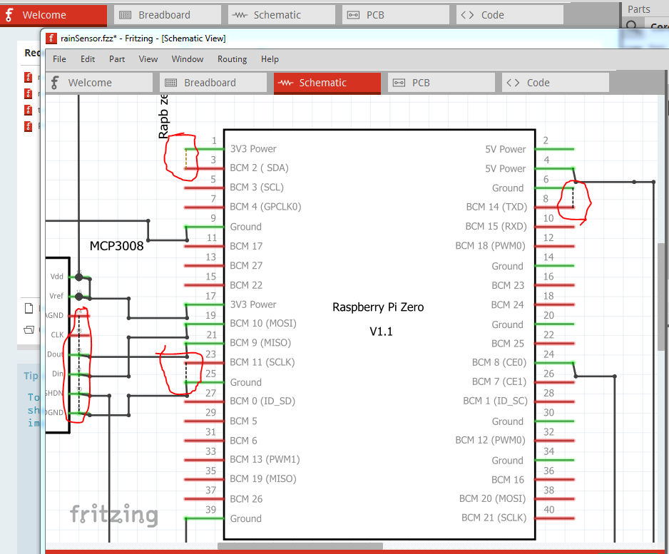
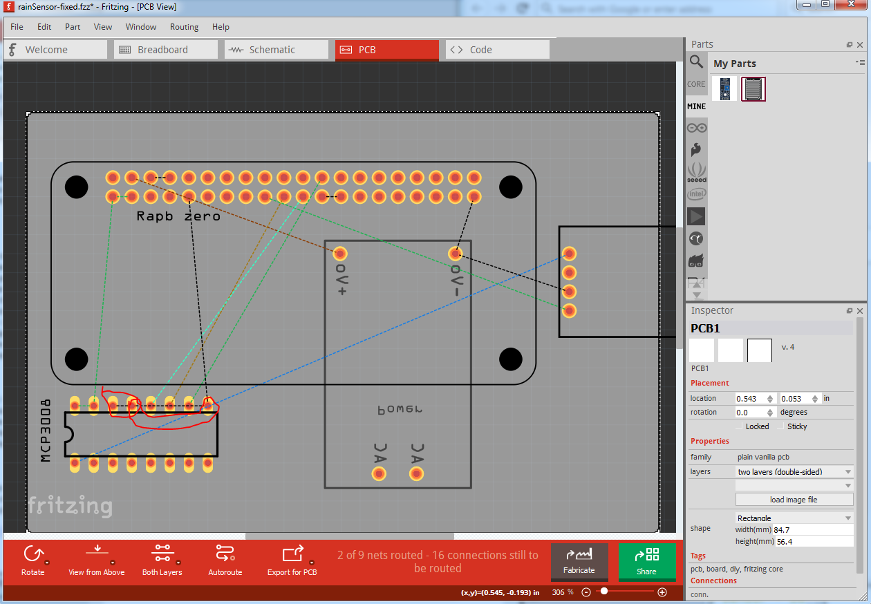
The first thing I’m going to do is delete minus the current parts (delete minus removes the part but leaves the connections so you can replace parts more easily.) Before doing that have a look at the traces in pcb circled in red in this image:
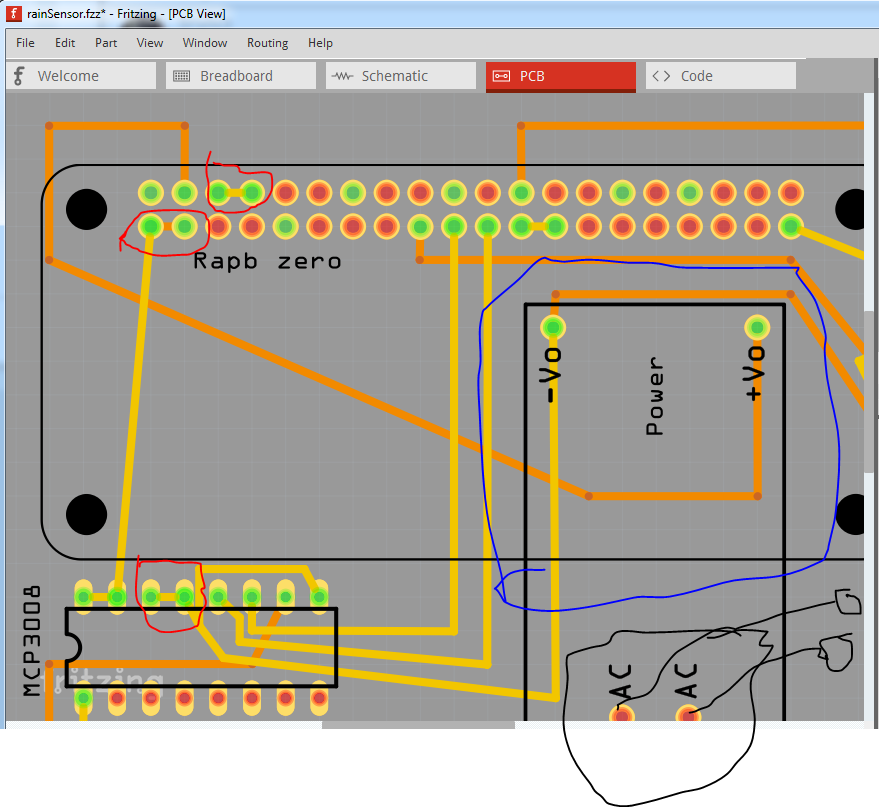
Note the red bar which indicates connector problems (probably from the bad part) but also the traces around the connections. They will be clearer below when the part is removed here:
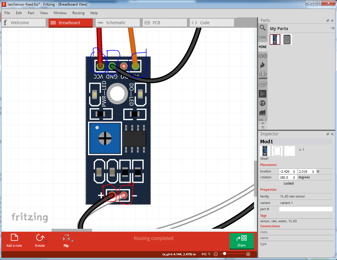
after the delete minus, we see the traces are not near where the connections were indicating a problem. Do the delete minus on the rain sensor part and switch to schematic (where the connecitons were correct) to see the parts (circled in red and blue) have been deleted but the traces are still there. The parts are at present still in the temp parts bin, so we need to save this sketch via file->Save as rainSensor-fixed.fzz to save a copy of the sketch without the two parts. Then close Fritzing and reload the sketch rainSensor-fixed.fzz via file open to get the sketch with the two old parts deleted. Then using File->Open load the two new parts in to the mine parts bin and drag the control board in to the sketch,rotate it 180 degrees (via right click rotate) and drag it on to the traces left from the last part. Here we see the top 4 traces reconnect (the connections are green indicating a connection):
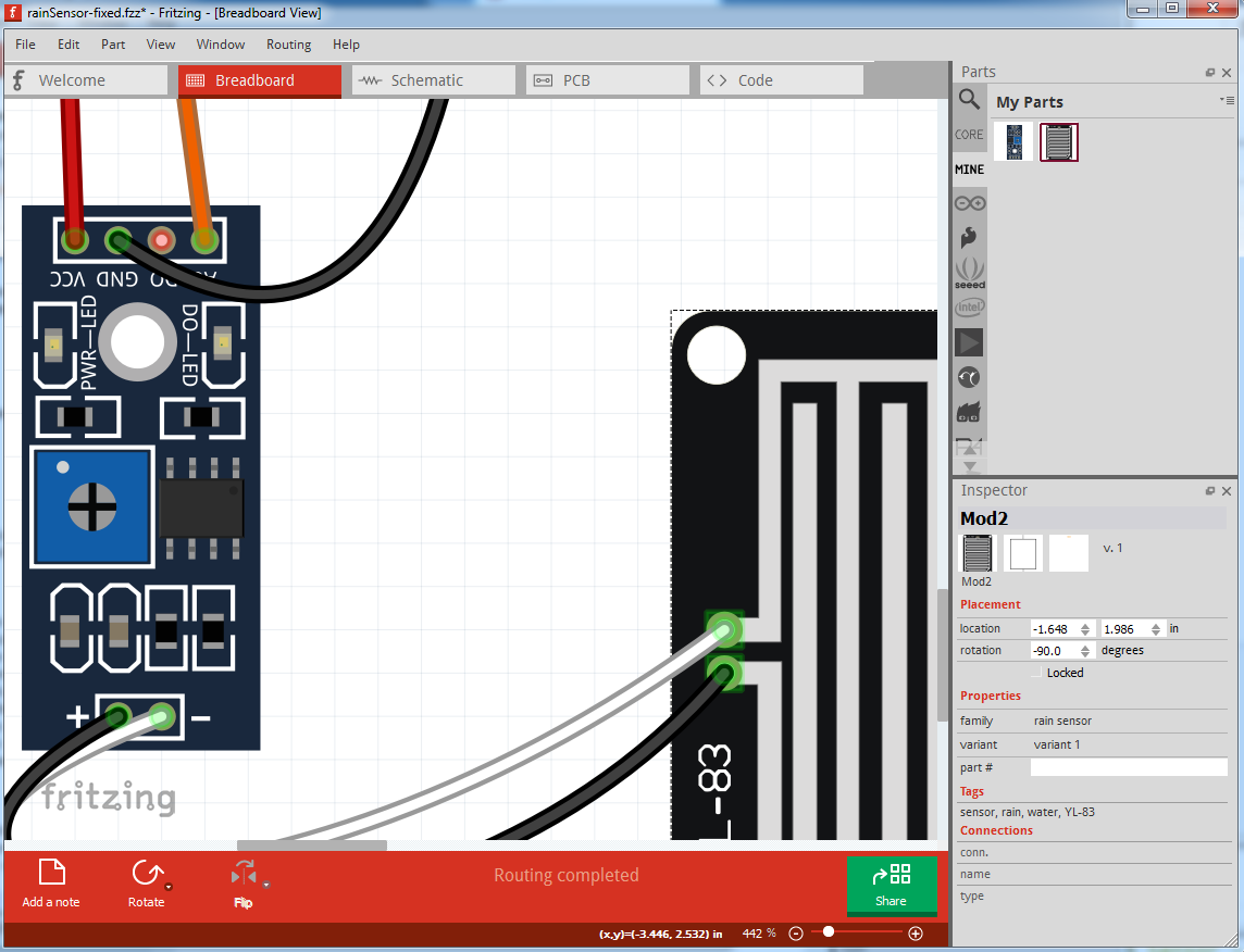
but the two to the sensor board (which isn’t in yet) are red indicating no connection. So drag in the new rain sensor board, rotate it 90 degrees clockwise and drag it until it touches the traces, both sets of connections are now green and breadboard is completed. Now on to schematic. Here as well we see the part is present but connected via rats nest lines, and not oriented correctly. We want to rotate it appropriately then drag it on to the connections as in breadboard then click on the end of the wire for any connection that is red and move it slightly so the connection re establishes and goes green like this. The wire circled in red was red til moved off the pin (upwards) then back on until it went green to indicate connected.
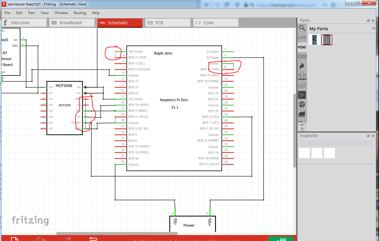
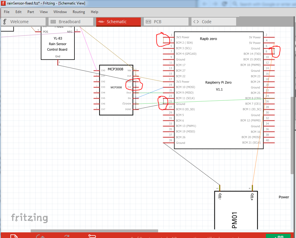
After a little pushing and pulling (you may want to check your View->Align to Grid setting, if it is not ticked click it to set align to grid so wires will snap to .1 boundaries as in this image) schematic is done. There are still some problems from the shorts in pcb which I haven’t removed yet. Circled in red in this image.
Now on to pcb. A couple of things to note: the new controller part has an outline in silkscreen. The traces for that part are not correct, so I will remove them and rerun traces according to the rats nest lines on the new part. As well I removed the wire to the power module, because I am going to select it and move it to the bottom of the board. While the traces will reroute when that happens it is usually easier to delete the traces then reroute once the part to be moved is changed and re oriented. This image is with all the traces removed. Not on the lower right (circled in red) that the power unit is set to be on the top of the board at present as is usual for parts. We are going to change that to bottom so it will be on the opposite side of the board from the Zero so both can be present at once without problems (if you can’t move the power unit to not overlap the Zero due to case constraints, it would be preferable to have all components on the top of the board.)
Here I have moved the power unit to bottom of the board and rotated it 180 degrees. Note that the text is now reversed because it is on the botto m of the board (and thus on the bottom silkscreen layer) and we are looking at the top. Also note the trace routing has gotten easier with this change. At this time I am going to remove the 3 traces that I believe shouldn’t be in pcb (circled in red) to see if that clears the problem in schematic with extra rats nest lines.
Unfortunately that does not clear the connection problems so we will need to try a bit harder. In pcb I selected Routing->Select all traces, then hit the delete key to remove all traces. That removes all the traces in pcb which looks like this:
Here we see the invalid connectiosn still exist as rats nest lines, so they are either in breadboard, or schematic or there is routing database corruption. Doing the same thing in schematic (Routing->select all traces) then delete indicates the problem is either in breadboard or database corruption because the undesired rats nest lines are still here.
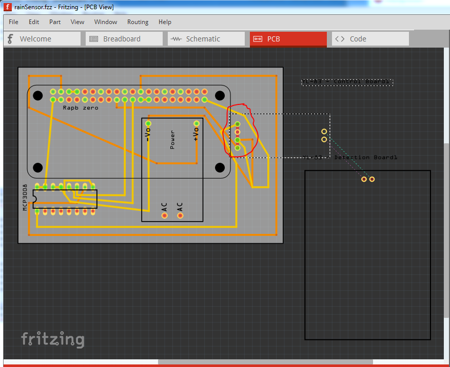
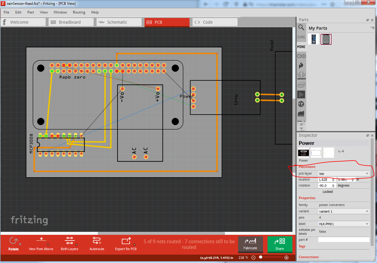
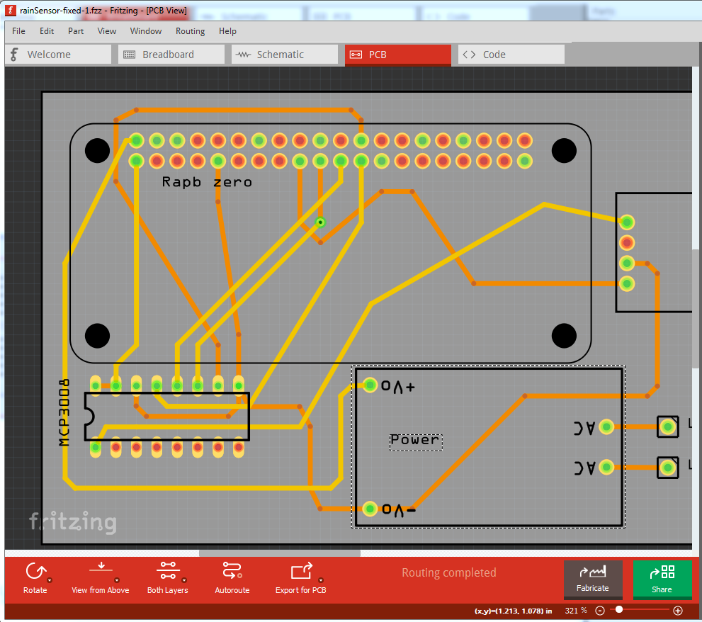
So now move to breadboard (the only remaining place other than database corruption) the connections may be. So if I hover over the yellow wire in breadboard the pin label says mcu pin 23 mcu pin 25. Since this should be only be pin 25 not also pin 23 there is a problem here. Removing the yellow wire, the pin now indicates it is pin 25 (ground) which should not be connecting to the clock pin on the MCP3008, pin 23 sclk seens a much more likely candidate, so move the yellow wire one pin right. This has the look of database corruption, so in breadboard do a Routing->Select all wires and press delete to delete all the wires. In theory this will reset the routing data base. First because of the dual row connectors on the Zero, in breadboard’s View->Set grid size change from the default .1in to 0.05in. This allows the wires to the dual row connector to come up between the pins so you can see where a wire connects easier. Now add the wires back in to breadboard and see what happens. First problem: there is a ground wire (the only one to the Zero) connected to Zero pin 8 which is bmc14 TXD, ground is pin 6, so assume pin 6 is correct and connect ground there instead of 8. Now add two single pin .1in headers to the AC power pins on the converter (which will appear as a pad in PCB which you can connect a wire rather than a connector to.) and breadboard is complete. You need to check either breadboard or probably easier schematic, to make sure I got everything connected correctly. Now move on to schematic and route all the rats nest lines. Note I chose to use ground symbols from core parts schematic view for the grounds rather than run wires every where (all the ground symbols connect together internally.) Now schematic is done. Then on to pcb. It is considered best practice to make connections with traces that are vertical, horizontal or at 45 degrees (no 90 degree bends) so thats what I did. I’d like to delete the one via, but I don’t see a way. As noted, the power supply mounts on the bottom of the board and the Zero on the top. If space isn’t a constraint, rotating the power supply so it is parallel to the Zero and on the top of the board would be a good bet. Here is the sketch these images are from and the two new parts (they are also in the temp parts bin of the sketch.)
YL-83 Rain Sensor - Control Board-fixed.fzpz (16.1 KB)
YL-83 Rain Sensor - Detection Board-fixed.fzpz (10.4 KB)
It would be good to offer these back to the place where you got the parts from if the person is still maintaining the site (the parts look to be made in 2016) to replace the current ones. Finally here is the sketch which assuming I got the connections right should do what you want (as noted you need to check that the connections are all as you expect.)
rainSensor-fixed.fzz (49.5 KB)
edit2:
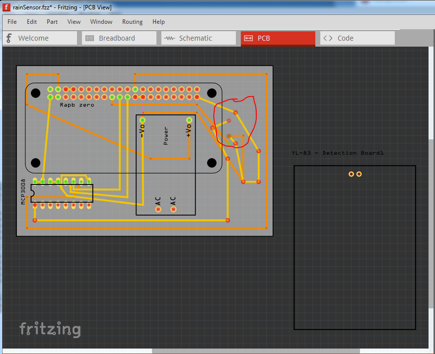
One more kick at the can before I call it a night. Here I swapped the power supply back to the top of the board. To do so I had to move the board down a bit (which you may not be able to do) in order to get enough room to put the power supply beside the zero:
and the sketch the above image is from:
rainSensor-fixed-1.fzz (50.3 KB)
Peter