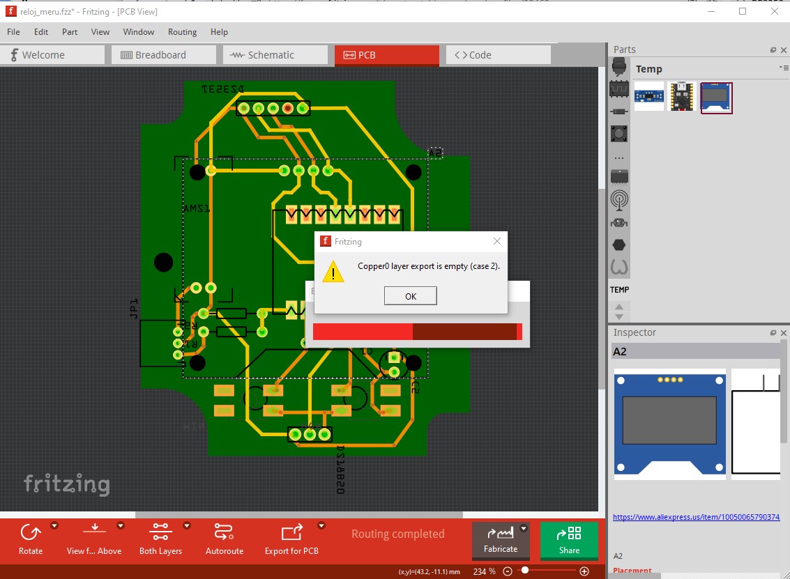
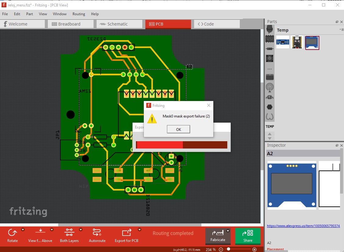
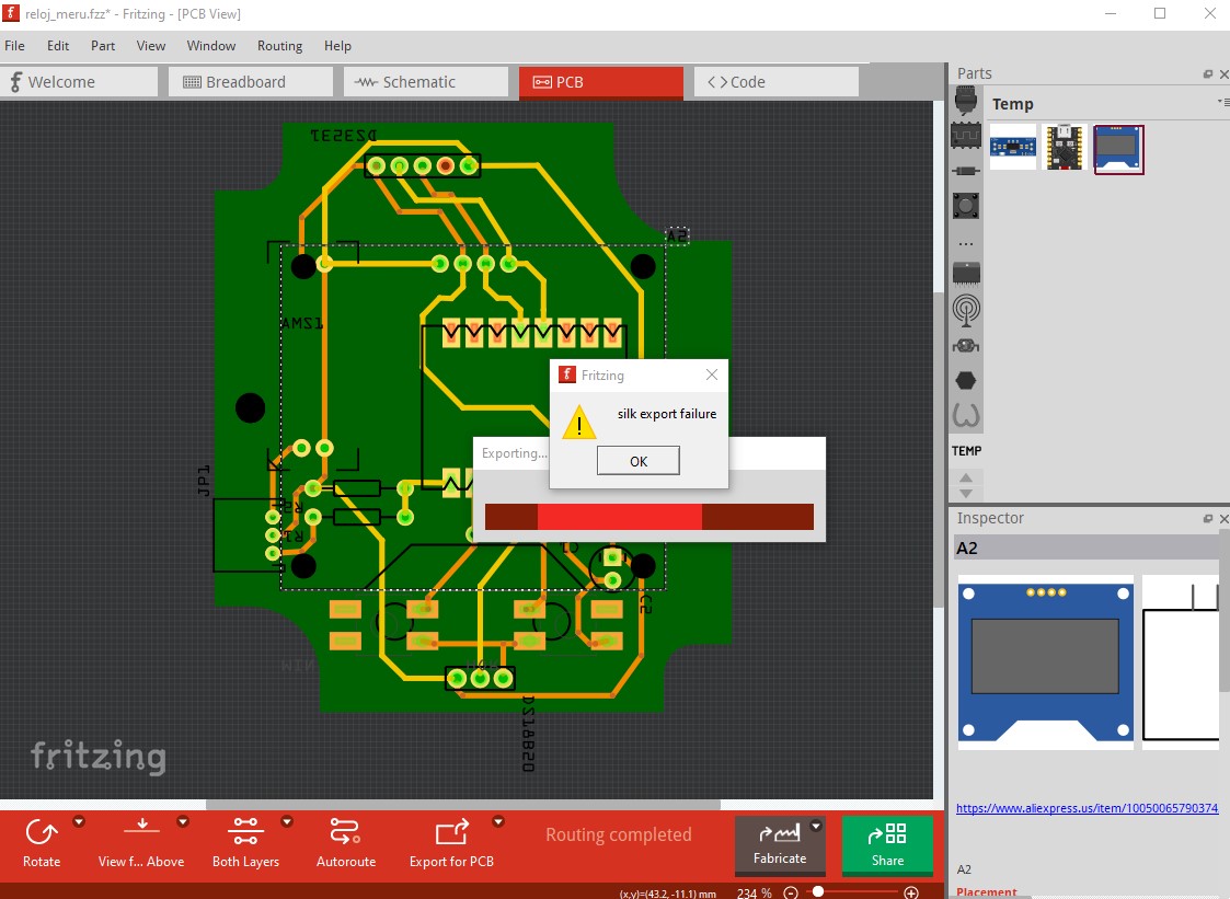
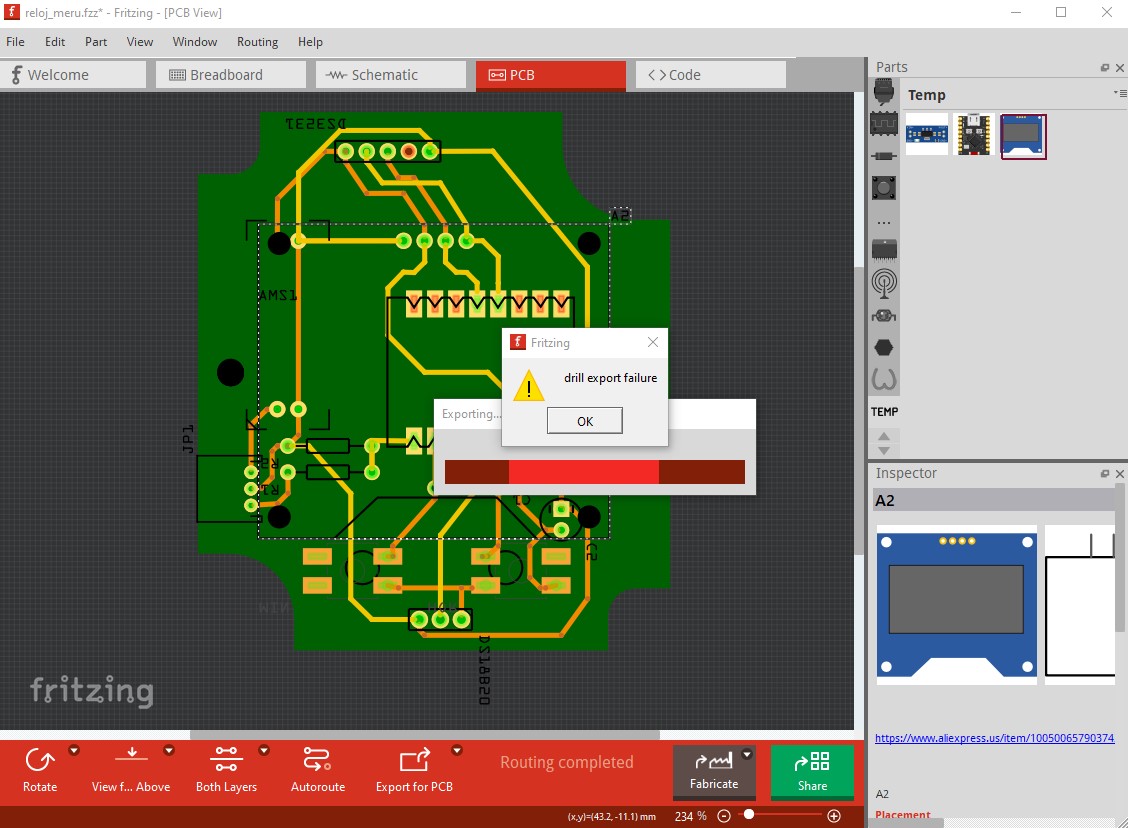
Hi, as the title says, when I export my board for etching or gerber files it comes up empty, I have google it and change almost everything on the board with out success
reloj_meru.fzz (70.0 KB)
I hope someone can help clarify this issue.
Hi, as the title says, when I export my board for etching or gerber files it comes up empty, I have google it and change almost everything on the board with out success
reloj_meru.fzz (70.0 KB)
I hope someone can help clarify this issue.
That is a real interesting (and really broken!) sketch. I wasn’t aware you could screw up a sketch badly enough to block gerber generation. But for me it indeed it screws up royally and generates almost nothing.
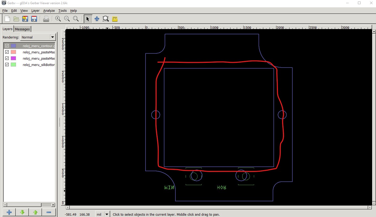
it generates gerber files for the contour.gml file (which may be the secret, it looks like there is a hole where the traces should go.) Two paste file (top and bottom with nothing in them and a silkbottom file (these are the generated gerber files displayed by gerbv)
I expect it can’t put copper in something that is milled out. I’ll need to recover the outline svg from the .fzz file and have a look at it.
Peter
ok, I figure it out, it was rh AMS1117 voltage regulator board, I just delete it and everything came back to normal.
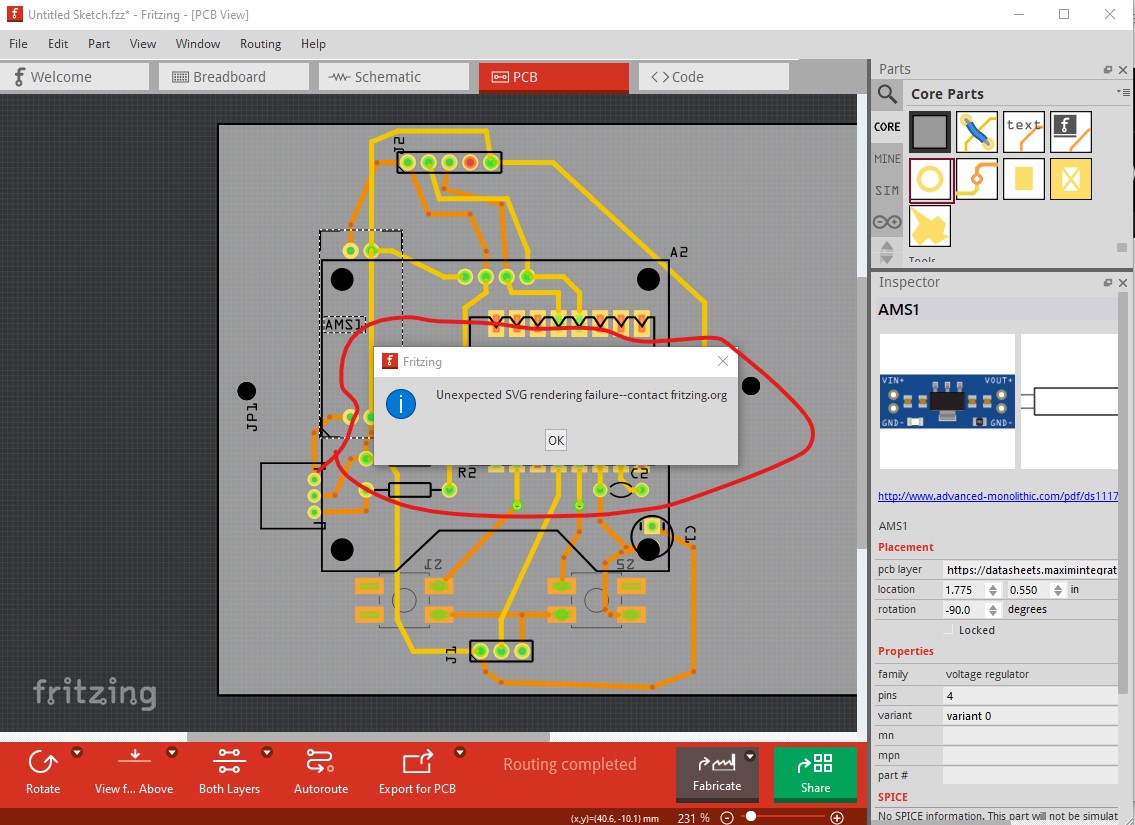
I just discovered the same thing. I am currently looking at what is wrong with the part. I don’t immediately see a problem, but there is one in there somewhere. It causes an interesting error
either this is new in 1.0.5 or I have just never run in to it before. I’ll figure out what is wrong and provide a corrected part.
Peter
Maybe can try with 1.0.4, 0.9.10, and 0.9.3b
The breadboard svg is filled with linear gradients (which Fritzing doesn’t support) I expect that is what is tripping the render error. It is likely easier to just make a proper part rather than fix this mess (certainly less work!) I’ll do that and upload it.
Peter
Even less work, someone cleaned up this part:
if you do a delete minus on the part it will delete the part bu leave the traces, You can then load the new part you may need to delete the old part if the moduleId didn’t change to load the new part though and then shutdown Fritizing answering yes to save parts and save parts bins then restart Fritzing (that is required to really delete the part!) then load the new one. You can then drag it in to the sketch and drag the traces to the new part to connect them.
Peter
OK here is an updated sketch with the fixed part installed. It now passes DRC and exports the gerber files correctly. I have mostly fixed the silkscreen labels, but I can’t select this one on the OLED display and it is currently off board and thus won’t show up. I don’t know what can be done to select it, Moving the part forward doesn’t help.
here is the corrected sketch
reloj_meru-fixed.fzz (61.3 KB)
Peter
Shifted topic to fab
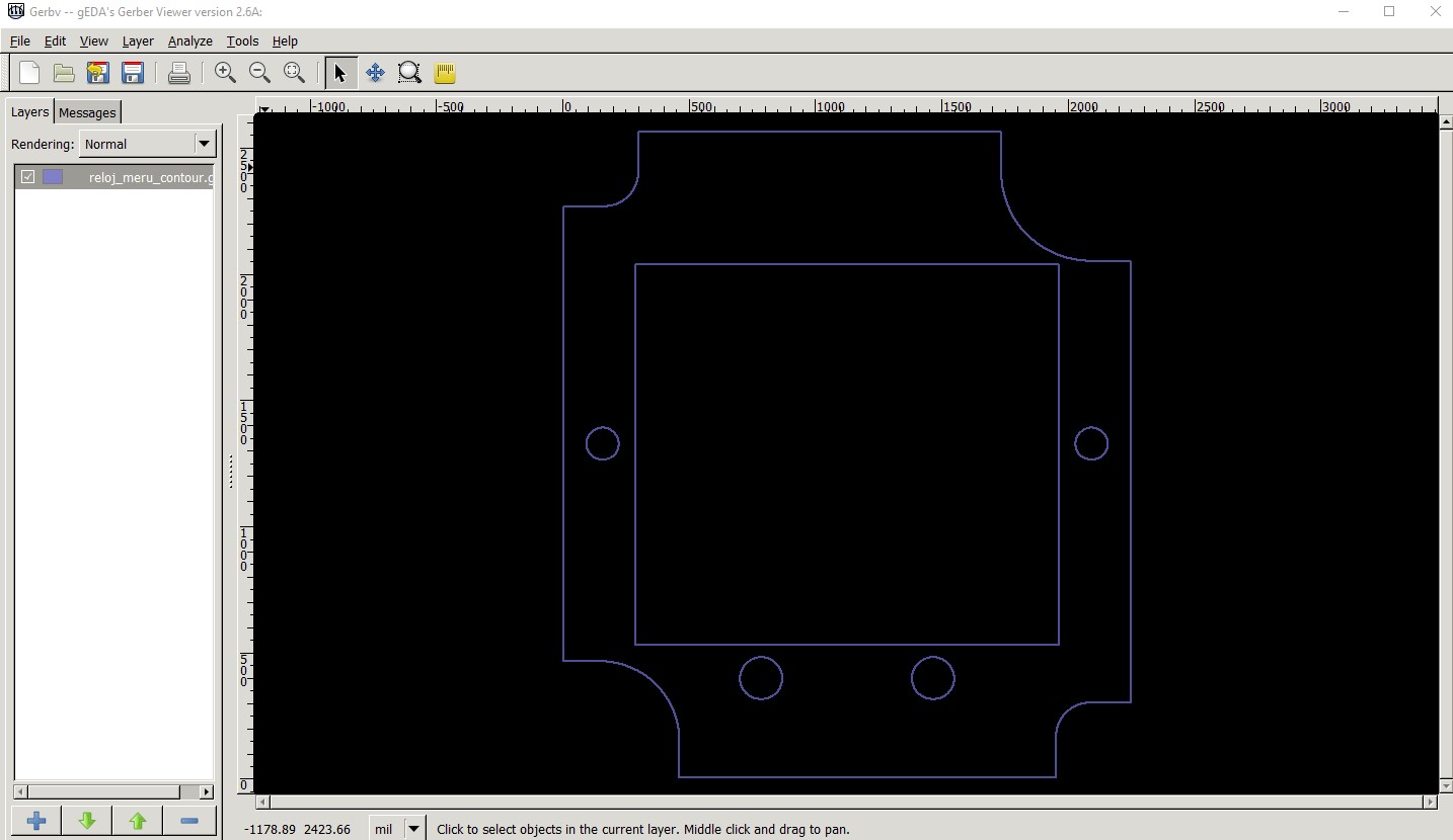
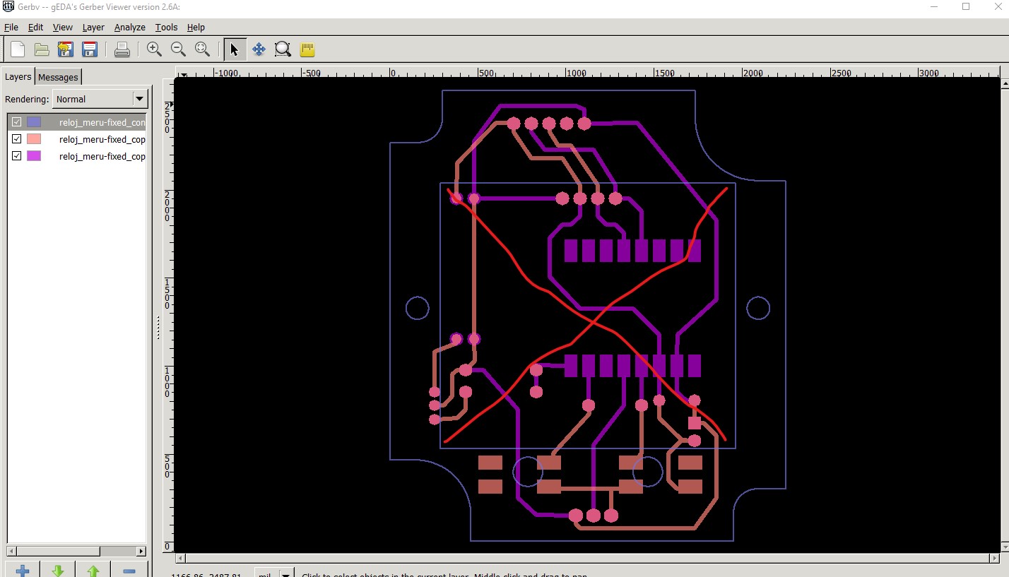
Even though the new sketch works, I still think from the contour.gml file that you are going to lose most of the traces as I think it is going to mill the a hole in the middle of your traces. Were you intending to have a slot in the center of the board (possibly for the LCD?) because is looks to me from the gerbers that you are going to get one.
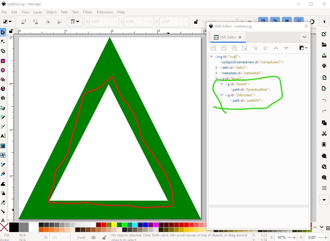
From other slots I have seen (although I’m not entirely sure) I think you are going to get a hole where the red X is. Since I think that will be milled out first there won’t be any traces there. This is the outline.svg file for a board that I know worked.
It cuts out the inner triangle (which I think is what your contour.gml file will do)
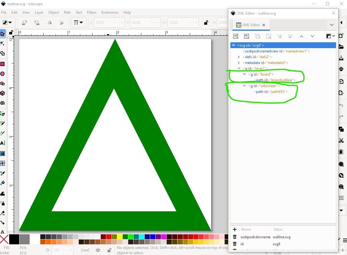
this is the associated outline.svg displayed in Inkscape
note there is a single path which is a difference of the paths that make up the image and the path (not a group as in your svg) is named boardoutline. Fritzing complains about no silkscreen (which is indeed missing in your svg) and that may mean the slots won’t be cut as I think they will be, but the contour.gml file appears as if it will cut the slot to me.
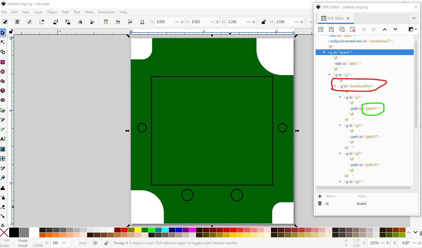
This is your svg (extracted from the .fz file) which is formatted incorrectly also displayed in Inkscape:
It is possible that you will get the slot in the center of the board and holes on the 4 circles (which will also interrupt traces) which would make the board not work. As noted that may not happen and you may only get the outline with no interior holes, but I don’t know for sure. I would fix up your outline svg to meet the slot standards before ordering boards though. I will also open a github ticket on the broken part breaking gerber processing so spectacularly as I expect the developers will be interested (from the please contact support in the error message!)
edit:
Looks like your outline.svg should work (mostly by accident!) when I load the outline file it tells me it found not cutouts despite what the contour.gml file says.
so as long as you didn’t want cutouts this may work.
Peter
Thank you for your observation @vanepp, I did draw the square in the middle and the 4 holes because the PCB is going to be in a tight space and I need to know where to center the display. I did try to make a silkscreen, but the instructions are not very clear on how to do it on Inkscape. If you could point me on the direction of a good tutorial it will be great.
I don’t think there are any. Most of us have learned by doing. A search in the forum search bar for “slots” should turn up past discussion there is an example circle.svg if I recall correctly in the part repository in pcb which has the necessary groups and there are in blog somewhere in how to do this. So you only want the circles on silkscreen on the outline svg? If so I can modify the copy I have to only cut the outline and add the necessary silkscreen stuff (silkscreen is more forgiving than the board outline usually.) The section in my parts tutorial is only for slots in parts, not general slot construction (and not what you want either.)
Peter
what I want to do is make the center rectangle and the 2 circles in the lower side to be silkscreen and the 2 circles on sides are holes for screws that will hold everything in place, the PCB need to have the wired shape that you see.
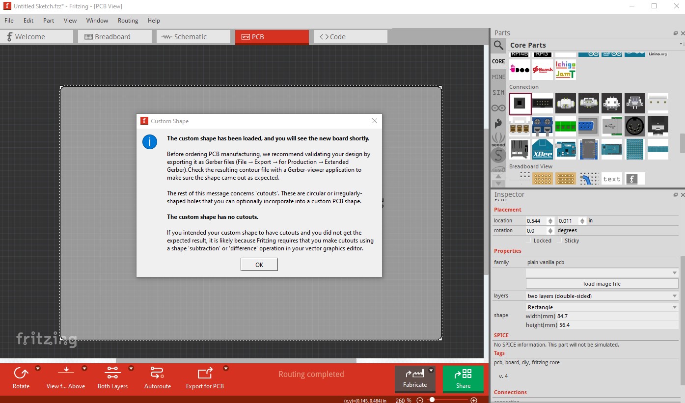
OK this svg should do what you want (and not cut a slot which I think the first one would have from the gerber output!) To download the svg right click on the image below and select save image as (which should default to outline.svg) and put it where ever you like.

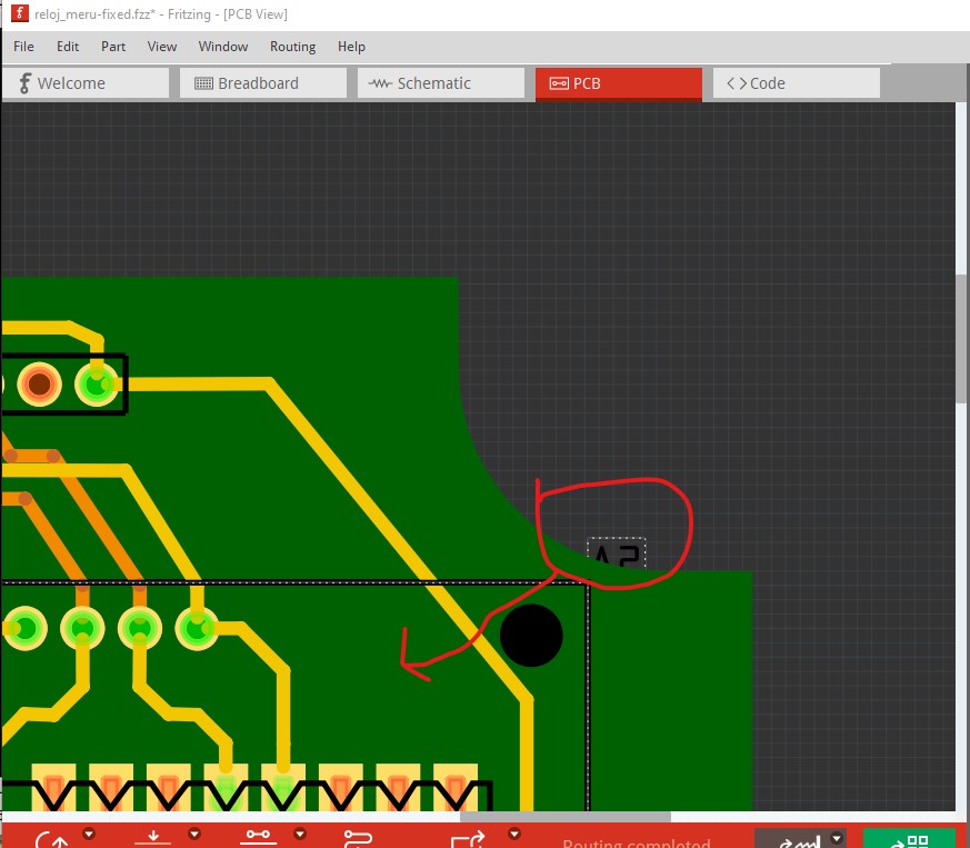
that gets you the new outline svg that you need to load as an image file in pcb view. Doing that should get this message from Fritzing
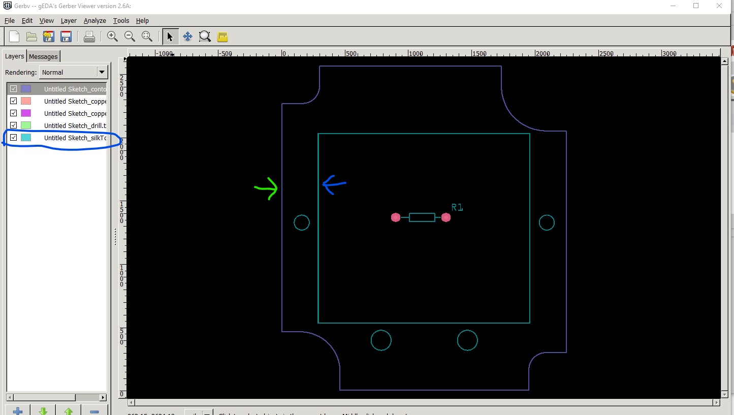
click OK and it should load your shape (you need to do this in the sketch with your board in it which should replace the current shape.) With that done and exported as gerbers it now appears to work correctly. The green arrow is the contour.gml file which cuts the board (no slots as the Fritzing message said!) The blue arrow is the silkscreen which has the square and circles (the resistor is only there to produce copper layers and will be replaced by the parts in your sketch in the real sketch.)
That should do what you want.
Peter