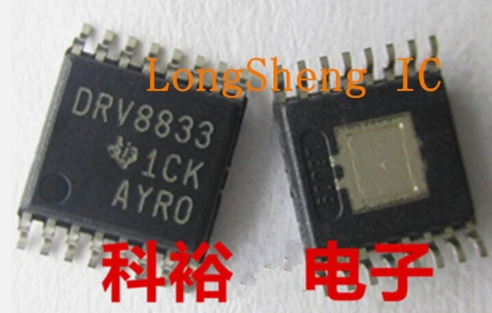
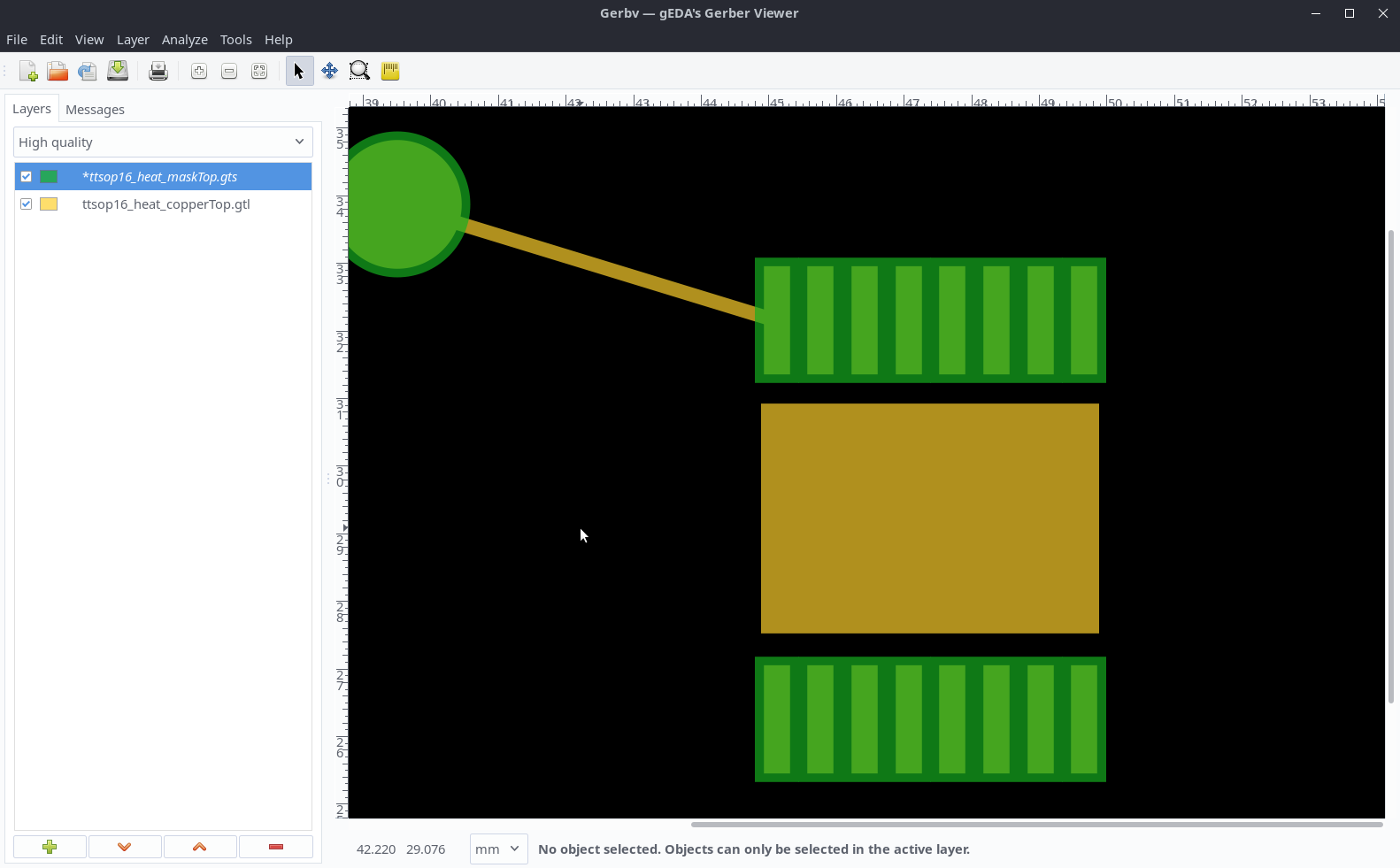
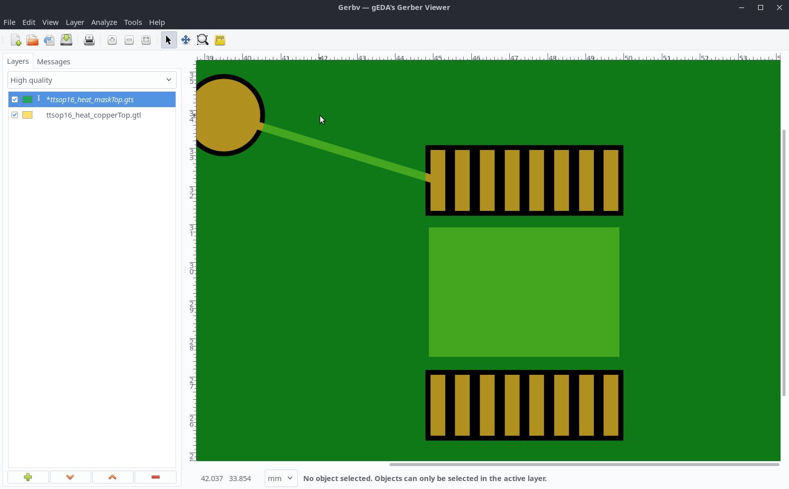
I was looking at the DRV8833 IC (not a board), it is a TSSOP16.
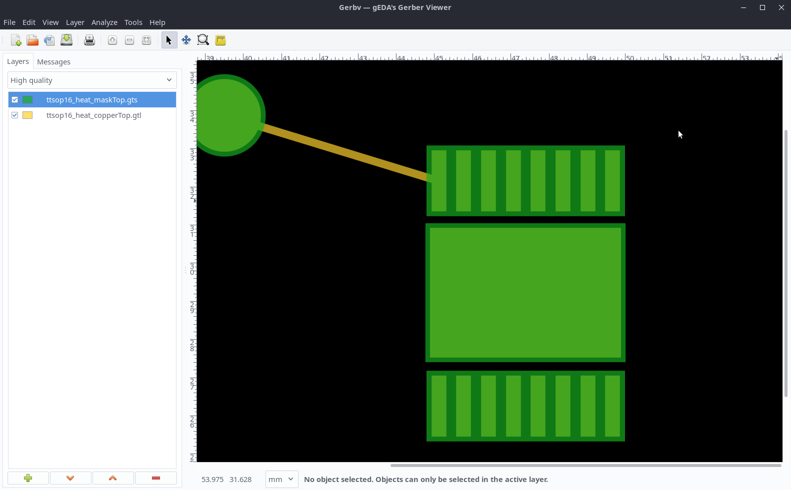
I could not find a Fritzing part for the DRV8833 hence I grabbed the first TSSOP16 part I could find and had a go at modifying the PCB part.
This is what I came up with so far:

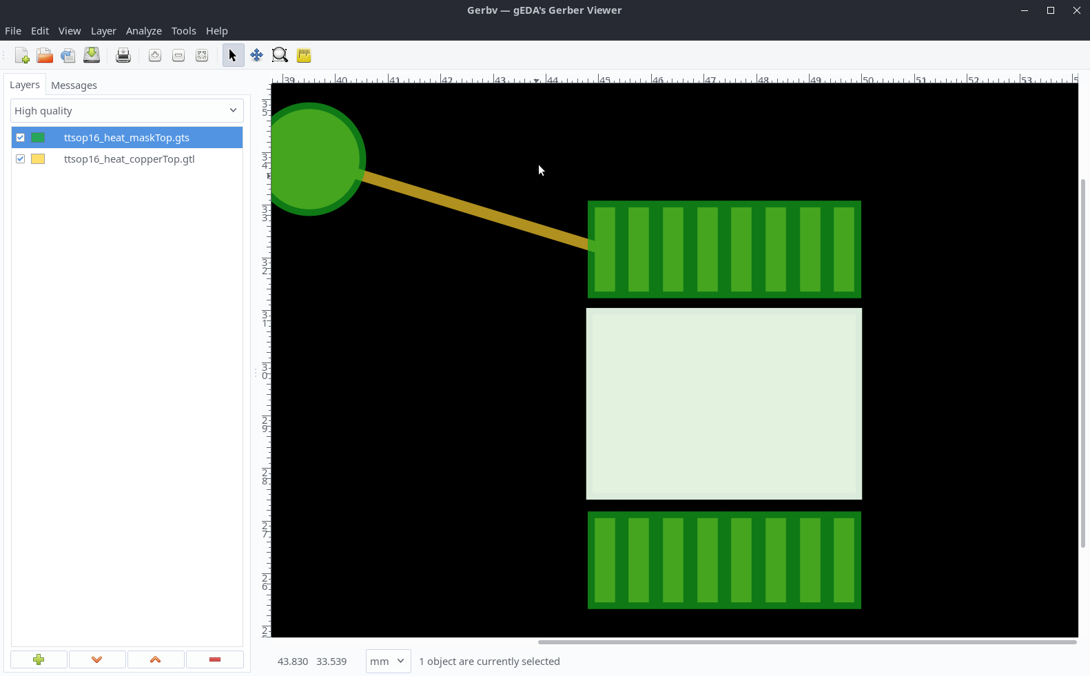
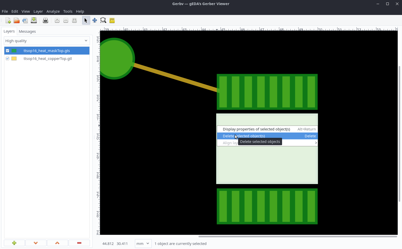
My issue is that only a part of the copper is supposed to be exposed and I have no idea how to do this, also the cooling pad should be both sides, can this be realised?
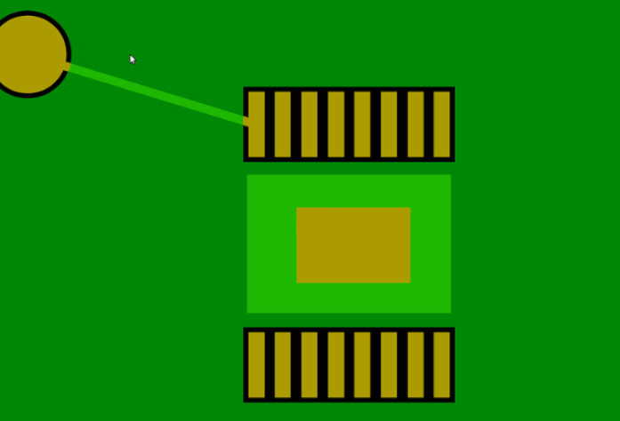
Maybe like this?
<g id="copper1" stroke-linecap="round" stroke-width="0">
<rect id="connector0pad" x=".114" y="5.8" width=".45" height="1.5" fill="#F7BD13" connectorname="1"/>
<rect id="connector1pad" x=".764" y="5.8" width=".45" height="1.5" fill="#F7BD13" connectorname="2"/>
<rect id="connector2pad" x="1.41" y="5.8" width=".45" height="1.5" fill="#F7BD13" connectorname="3"/>
<rect id="connector3pad" x="2.06" y="5.8" width=".45" height="1.5" fill="#F7BD13" connectorname="4"/>
<rect id="connector4pad" x="2.71" y="5.8" width=".45" height="1.5" fill="#F7BD13" connectorname="5"/>
<rect id="connector5pad" x="3.36" y="5.8" width=".45" height="1.5" fill="#F7BD13" connectorname="6"/>
<rect id="connector6pad" x="4.01" y="5.8" width=".45" height="1.5" fill="#F7BD13" connectorname="7"/>
<rect id="connector7pad" x="4.66" y="5.8" width=".4" height="1.5" fill="#F7BD13" connectorname="8"/>
<rect id="connector8pad" x="4.66" width=".45" height="1.5" fill="#F7BD13" connectorname="9"/>
<rect id="connector9pad" x="4.01" width=".45" height="1.5" fill="#F7BD13" connectorname="10"/>
<rect id="connector10pad" x="3.36" width=".45" height="1.5" fill="#F7BD13" connectorname="11"/>
<rect id="connector11pad" x="2.71" width=".45" height="1.5" fill="#F7BD13" connectorname="12"/>
<rect id="connector12pad" x="2.06" width=".45" height="1.5" fill="#F7BD13" connectorname="13"/>
<rect id="connector13pad" x="1.41" width=".45" height="1.5" fill="#F7BD13" connectorname="14"/>
<rect id="connector14pad" x=".764" width=".45" height="1.5" fill="#F7BD13" connectorname="15"/>
<rect id="connector15pad" x=".114" width=".45" height="1.5" fill="#F7BD13" connectorname="16"/>
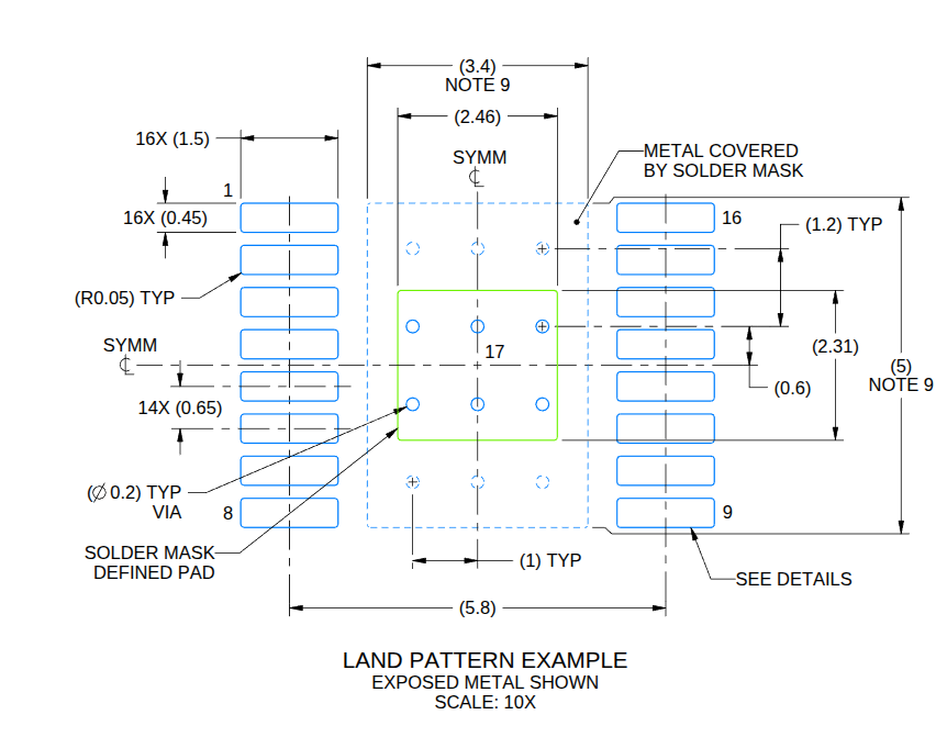
<rect id="connectorHeatPadT" x=".114" y="1.9" width="5" height="3.4" fill="#f7bd13" connectorname="17"/>
<g id="copper0">
<rect id="connectorHeatPadB" x=".114" y="1.9" width="5" height="3.4" fill="#f7bd13" connectorname="17"/>
</g>
</g>
I had a look how the ATMEGA1284 realises the vias and tried to copy the concept. But I could not see a bottom pad.
Footprint
TSSOP16 with cooling pad
Type
I did not read this
Breakout board, sub assembly, plug in module (A)
Antenna (AE)
Battery (BT)
Capacitor (C)
Diode (D)
Display (DS)
Fuse (F)
Hardware , mounting screws, etc. (H)
Jack, fixed part of a connector pair, header (J)
Relay (K)
Inductor, Coil, Ferrite bead (L)
Loudspeaker, Buzzer (LS)
Motor (M)
Microphone (MK)
Plug, moveable part of a connector pair (P)
Transistor (Q)
Resistor (R)
Thermistor (RT)
Varistor (RV)
Switch (S)
Transformer (T)
Integrated Circuit (IC)
Crystal, Oscillator (Y)
Zener diode (Z)
Other (please specifiy)