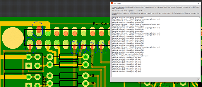
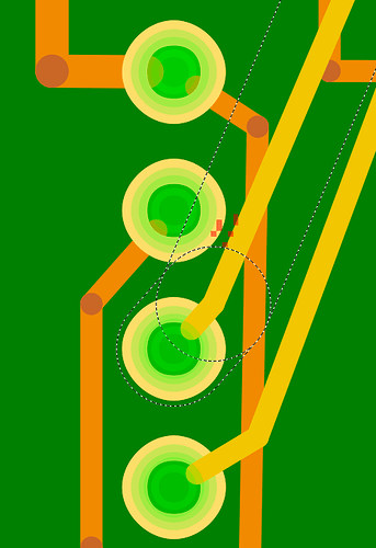
It is not the trace thickness causing the problems. I Narrowed one of the drc complaining traces to 8 mil and it still complained. However, when I added a via, and moved the complaining piece to the top board layer, it quit complaining even at 48 mil. Looking over the drc results ALL of the complaints (for the header part) are for the bottom layer. Which gives a place to look in the part definition and svg. If all of the copper0 is nested inside of copper1, it should not be an svg problem.
I have been doing some working on a couple of issues with drc, and this initially looked potentially similar. I ran your file through my development version, that fixes some things, and got the same (at least close) complaints. After checking for top versus bottom differences, if nothing shows up, I can run a slower debug test to find out the state in drc for the complaints. Tracing what is happening in drc is all set up, because of the other fix I was working on.
There are some unrelated drc complaints on other parts of the board that look real. Probably will get handled by that “tidy up” you mention, but here are some screenshots. I hope I left enough around the zoomed sections to match to the full board.

I extracted your part from the sketch file, and ran it through a checking (validation) tool. It did not complain about anything in the definition file and my quick scan did not notice any obvious problems. The relevant complaints are:
Warning 20: File
'…/svg.pcb.RaspberryPi Connector and Hat_00e45d2c131e75a2568c29ffe4cebaff_2_pcb.svg'
At line 28
copper1 layer should be at the top, not under group copper0

Warning 25: File
'…/svg.pcb.RaspberryPi Connector and Hat_00e45d2c131e75a2568c29ffe4cebaff_2_pcb.svg'
At line 122
Silkscreen layer should be above the copper layers for easier selection
in pcb view

Warning 23: File
'…/hat/svg.pcb.RaspberryPi Connector and Hat_00e45d2c131e75a2568c29ffe4cebaff_2_pcb.svg'
At line 124
Key -inkscape-font-specification
value 'Droid Sans, Normal' is invalid

Error 69: File
'…/hat/svg.pcb.RaspberryPi Connector and Hat_00e45d2c131e75a2568c29ffe4cebaff_2_pcb.svg'
At line 19
Found a drawing element before a layerId (or no layerId)
Only the last of that is considered to be an error by the tool, but it prompted a closer look at the svg file. Which discovered likely problems the tool was not noticing.
Warning 20:
    <g transform="translate(27.228583,7.6328196)" >
        <g >
            <g partID="858626900"  gorn="0.4.0.0" id="copper0">
                <g transform="translate(-0.84937993,0.42607221)" >
                    <g >
                        <g  gorn="0.4.0.0.0.0.0" id="copper1">
Having copper1 inside of copper0 is only a warning, but I also see that there is a transform between them. the copper1 layer is shifted a little relative to copper0, which I think could cause problems. There is nothing in cop0 that is not in copper1, so it should not be too bad. The transform around both copper layers is valid svg, but there are multiple reports that in some conditions Fritzing is not handling them properly. I also see a partID in there, which is not expected in a part itself. It is used in a sketch to track (potentially) multiple copies of a single part. I assume that got in there because you pasted something into Inkscape that that was exported from a Fritzing sketch. Cleaning up the groups and transforms described below will get rid of that too.
Warning 25: Self explanatory. The silkscreen layer/group is at the bottom of the svg file instead of the top. It also has an unneeded transform around the group.
Warning 23:
<g stroke-width="1.0004" stroke="none" xmlns:xml="http://www.w3.org/XML/1998/namespace" fill="#000000" font-size="2.39999" gorn="0.5.0.0.1" xml:space="preserve" fill-opacity="1" id="1Silk" style="font-style:normal;font-variant:normal;font-weight:normal;font-stretch:normal;line-height:1.25;font-family:Droid Sans;-inkscape-font-specification:'Droid Sans, Normal';font-variant-ligatures:normal;font-variant-caps:normal;font-variant-numeric:normal;font-variant-east-asian:normal;stroke-miterlimit:4;stroke-dasharray:none">
Somehow you got inkscape to specify the font strangely. At least strange for Fritzing, according to the checker tool.
Error 69:
    <g transform="matrix(1.0429448,0,0,1.0322221,-26.614969,1.3818347)" >
        <g >
            <g stroke-width="0"  gorn="0.3.0.0" style="stroke-miterlimit:4;stroke-dasharray:none" id="board">
                <rect stroke-width="0" stroke="none" rx="8.5301027" y="-1.338699" stroke-opacity="1" fill="#008000" height="160.65027"  gorn="0.3.0.0.0" ry="8.5301027" width="184.81889" x="25.518803" fill-opacity="1" id="rect2424" style="stroke-miterlimit:4;stroke-dasharray:none;stroke-dashoffset:0;"/>
            </g>
        </g>
    </g>
I have never used a board layer in a part. I do not know quite what is valid. Can definitely do without that wrapping transform. Did that maybe get carried in from wherever that partID came from? Or did you created it deliberately?
To get rid of all of the transforms, select the pieces and ungroup them. Multiple times to unwrap the various groups/layers. That will also remove layer definitions, so those need to be added back in after all the unwrapping. Before adding those back in, select everything in the drawing (as a block), and move it to coordinates 0,0. Then add only the needed groups back in.
<svg xmlns="http://www.w3.org/2000/svg" version="1.2" y="0in" height="58.499996mm"  gorn="0" width="68mm" x="0in" viewBox="0 0 192.75534 165.82675" id="svg261">
>>> 192.75534/68
2.834637352941176
>>> 165.82675/58.499996
2.834645492967213
>>> 165.82675/58.499996*25.4
71.99999552136721
Your svg file dimensions are a little odd. Those values translate to about 2.83 pixels per mm, which is 72 px per inch. So fairly normal after converting through mm.
