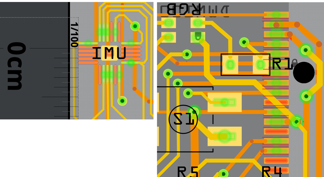
I have a custom made part for the MPU9250 9-axis motion sensor. It is a 3mm 24-QFN package, so quite small.
Additionally I use a Decawave DWM1001, which is - kind of - SMT package.
See the datasheet: https://www.decawave.com/sites/default/files/dwm1001_datasheet.pdf
The MPU9250s pads are some 0.18mm, the DWM1001’s pads are 0.35mm apart.
Below are 2 images showing the details of the 2 elements (DWM1001 only right half):
For both MPU and DWM I get DRC overlapping errors for every pad that has a connected trace and their neighboring pads - Why? It doesn’t matter how thin I set the traces.
The DRC error basically tells you a human eye needs to check them because there might be contact. If you can see gaps and the gap is wide enough for min width manufacture - I think it’s 0.006"(0.15mm) for most houses - it should be ok. You can print it out an check.
That being said, where did the part come from. Like is it made properly. I’m see orange traces with red spots, and that means the bottom layer copper is close, which is weird when a SMD only has a top layer. Is this a double loaded PCB.
Thanks for the hints!
It is a double layered PCB with the MPU9250 on top and the DWM1001 on the bottom side. Both are custom made parts by myself. Could it be a faulty SVG?
If the IC foot print is only on one side they should be ok, it’s just that I thought there might be an error in that part where pads were on both sides.
The usual procedure is to print it out an check parts fit on it, because you don’t want to get it made and find out it’s wrong.
I have found that Fritzing does not deal well with individual parts that have tight spacing when checking with the the DRC tool. It almost seems that it ignores the settings and uses the default spacing when checking between pads on a single footprint. All I have done is made sure it looked exactly as I intended before sending them off to have manufactured.
What you will find when you get the boards back from your manufacturer is that the spacing is so tight that you will not get any solder resist between the pads but otherwise they will be exactly what you have designed.