DRC check problem

Hello, Peter can you check this problem…

I was Modifying one of my old part…
After hours of editing every view, I just faced a very new problem in DRC…

There are invisible Copper pad appears in that part…
I only edited the design, Tried new creation / edit over core file… Also edited on inkscape, But problem still same…

I make the trace thicker to see full GHOST copper pads… :sweat_smile:

Here is the screenshot in short…

Here is the file, 42. 7 Segment Display CC.fzpz (28.9 KB)

I submitted this part before, that was working good…
I didn’t find any error in svg xml…
Also, checked everywhere if old part file left anywhere, but nothing…

Is this only happening on my PC…!!! :cold_sweat: :cold_sweat:

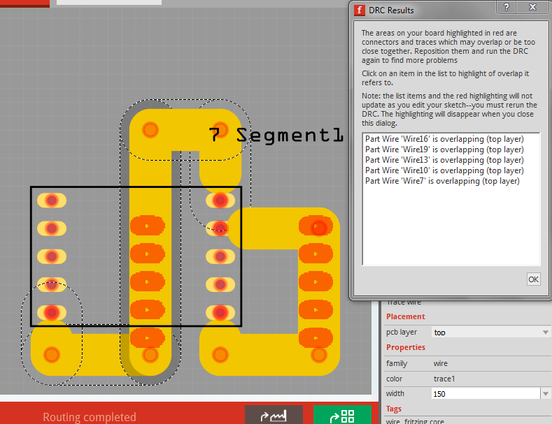
The (probably) fix for this is sitting in a code pull request. I created https://github.com/fritzing/fritzing-app/issues/3647 because some elongated connector pads were not being detected as drc collision candidates. The fix, if/when accepted will only be helpful if you are running the lasted development version, but there is a simple patch for the svg file. In svg path elements, It is valid to have a negative number immediately after another number without an intervening comma or space. However the existing code does not handle that for some graphic commands. Looking at the svg.pcb.AG_7_Segment_51b1fec2575b089cc5c4776d5dd9f773_2_pcb.svg file from your part I see (in part)

d="M10.391,20.622c1.034,0,1.872,0.838,1.872,1.871l0,0v3.744c0,1.033-0.838,1.871-1.872,1.871l0,0l0,0
	c-1.034,0-1.872-0.838-1.872-1.871l0,0v-3.744C8.519,21.46,9.357,20.622,10.391,20.622L10.391,20.622z M9.24,24.364
	c0,0.639,0.515,1.152,1.15,1.154c0.637,0,1.152-0.516,1.152-1.152c0,0,0,0,0-0.002c0-0.635-0.516-1.15-1.151-1.15
	C9.755,23.212,9.24,23.728,9.24,24.364L9.24,24.364z"

In that, I suspect “0-1.872-0.838-1.872-1.871” (and similar) will cause the same silent failure I saw. Simply replacing all of the “-” characters in the d attribute strings with " -" with a text editor should work around the problem. This has not been tested, but fits the pattern I saw. That edit probably needs to be the last step, since I suspect that Inkscape, or other svg editors, will remove the extra spaces again.

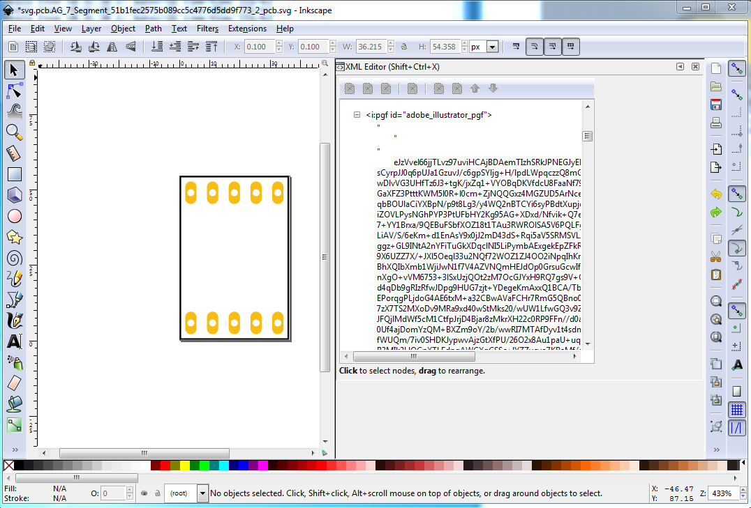
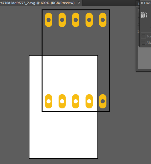
That should be a fairly simple test, to see if that really is the cause anyway. The svg file seems valid, though it contains unexpected (for me) content. It might not be valid for the tiny svg used for Fritzing. The pieces that look suspicious to me are the switch, foreignObject, and i:pgf elements. None of that should be needed for pcb image. At least visually the pcb image looks the same without that content.

There is also information around the documentation and forum about not using size in px for Fritzing parts. That often cause problems. Size needs to be specified in real world units’

width="36.415px" height="54.558px" viewBox="6.584 -24.514 36.415 54.558"

I do not have the scaling exact, but changing that to

width="0.4in" height="0.56in" viewBox="6.584 -24.514 36.415 54.558"

looks close in my image viewer (at 10 times scale). The forum does not want to upload the svg image, as reported in other places, so here is my quick (untested) adjustment to the pcb svg back in the part file.

part.fzpz (7.3 KB)

Notice that the part file is much smaller now, because the pcb image is much smaller without the embedded pdf. This did NOT add the spaces mentioned first. If this looks/works reasonable, fine. Otherwise try adding the spaces too.

I expect Phil has the right of it, as everything I have tried fails.

Fritzing check part has a number of complaints:

Warning 36: File
‘part.AG_7_Segment_51b1fec2575b089cc5c4776d5dd9f773_2.fzp.bak’

Connector0 doesn’t exist. Connectors should start at 0

Warning 35: File
‘part.AG_7_Segment_51b1fec2575b089cc5c4776d5dd9f773_2.fzp.bak’

Connector0 doesn’t exist when it must to stay in sequence

Warning 19: File
‘svg.breadboard.AG_7_Segment_51b1fec2575b089cc5c4776d5dd9f773_2_breadboard.svg.bak’
At line 6

Height 53.857px is defined in px
in or mm is a better option (px can cause scaling problems!)

Warning 19: File
‘svg.breadboard.AG_7_Segment_51b1fec2575b089cc5c4776d5dd9f773_2_breadboard.svg.bak’
At line 6

Width 35.717px is defined in px
in or mm is a better option (px can cause scaling problems!)

Warning 19: File
‘svg.schematic.AG_7_Segment_51b1fec2575b089cc5c4776d5dd9f773_2_schematic.svg.bak’
At line 6

Height 44.182px is defined in px
in or mm is a better option (px can cause scaling problems!)

Warning 19: File
‘svg.schematic.AG_7_Segment_51b1fec2575b089cc5c4776d5dd9f773_2_schematic.svg.bak’
At line 6

Width 44.182px is defined in px
in or mm is a better option (px can cause scaling problems!)

Warning 34: File
‘svg.schematic.AG_7_Segment_51b1fec2575b089cc5c4776d5dd9f773_2_schematic.svg.bak’
At line 60

translates are undesirable.

Warning 19: File
‘svg.pcb.AG_7_Segment_51b1fec2575b089cc5c4776d5dd9f773_2_pcb.svg.bak’
At line 16

Height 54.558px is defined in px
in or mm is a better option (px can cause scaling problems!)

Warning 19: File
‘svg.pcb.AG_7_Segment_51b1fec2575b089cc5c4776d5dd9f773_2_pcb.svg.bak’
At line 16

Width 36.415px is defined in px
in or mm is a better option (px can cause scaling problems!)

Error 69: File
‘svg.breadboard.AG_7_Segment_51b1fec2575b089cc5c4776d5dd9f773_2_breadboard.svg.bak’
At line 7

Found a drawing element before a layerId (or no layerId)

Error 89: File
‘svg.pcb.AG_7_Segment_51b1fec2575b089cc5c4776d5dd9f773_2_pcb.svg.bak’
At line 16

ViewBox ‘6.584 -24.514 36.415 54.558’

has characters other than 0-9, whitespace or ‘.’ or not four values.
It must be dimensionless and have 4 numeric values

The view box (which I don’t think you can modify in Illustrator) is not origined at 0 0 and the drawing is in px which makes it incorrectly scaled in Inkscape. So ungroup the svg. edit select all and resize page to drawing to set the view box to origin at 0 0 then rescale to get the pads on .1 boundaries as before (change display units from px to pt change scale from 1.33333 to 1.)
Change display units back to px and Units to in to avoid the scaling issue and edit select all resize drawing to reset the view box again. Now regroup (and the Illustrator oddness is gone as well.) and save as plain svg.

but the result still fails DRC, I expect because of the bug that Phil mentioned.

Peter

Thanks Merlin & Peter…

The github article is useful, I familiar with some of the problems,
the “translate” node causes problem some time, I checked that… No issue.

The “translate” part actually created by inkscape. That’s another reason I use AI…

I tried with separate copper layer, no help…

I Checked your new svg, after opening in AI, Artboard changed location… That’s where those invisible pads are appearing…!!!

Anyway, I relocate them… Now the part is working fine… But with smaller size…!!

Without wasting any time, I made a new fresh copy of the pcb, with minimum relocating the paths…
Now, the part successfully passed in one try…!!!

That’s my fault I never use grid setting, so, I move every path so many times…!!

Thanks both of you to locate the real issue…

If you want to check, 42. 7 Segment Display CC .fzpz (6.7 KB)