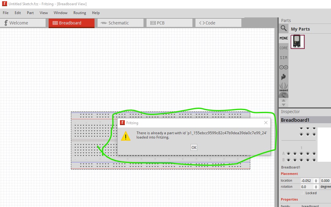
After downloading .fzz file > File > Open > There is already a part with ‘p1_155…’ loaded into Fritzing.
Did already re-install Fritzing after deleting all files (?)
After downloading .fzz file > File > Open > There is already a part with ‘p1_155…’ loaded into Fritzing.
Did already re-install Fritzing after deleting all files (?)
Your best bet is to upload the .ffz file (upload is 7tth icon from the left in the reply menu) so we can try uploading it.
Or specify the complete name of the part it is complaining about (as “There is already a part with ‘p1_155…’ loaded into Fritzing.” isn’t enough information to do anything with"). Reintstalling Fritzing won’t help because there is a problem in the .fzz file you wart tyrint to load not Frtizing.
Peter
The message seems to be saying that a part in the Fritzing (sketch) file conflicts with a part already loaded into the app. Not enough information to tell if that is a core part, or a custom part (in your “Mine” parts bin). If it is in “Mine”, you could fix it by deleting that part from there, exiting (with save for parts bin changes), restart Fritzing, then open the fzz.
Thanks MicroMerlin. Did not work.
Peter: hope it will help!
NodeMCU-WROOM-ESP32_30pol.fzpz (222.4 KB)
You said fzz to start with, which is a sketch file. What was uploaded was a part file. Quite different case. That part file loads just fine on my system.
Assuming the original message was incomplete, there is another part on your system that has the same ID as that part. Fritzing can only load a single part with a specific ID.
Also loads fine for me on 1.0.4. Looks like you probably already have such a part loaded. Try this search in the parts bin and see if something comes up. The fzp file has no tags so this may or may not work depending on how search works.
For you hopefully a part will appear like this (with your part loaded) although it does not for me
plan B reduce the search to nodemcu then it appears as it should
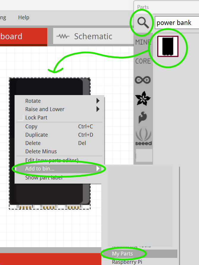
If you get a hit you need to remove that part before the new one will load. Note when you remove the part you then need to shut Fritzing down (answering yes to save the part, and to save the parts bin) before it will be really deleted on restart.
edit
attempting to load the part again causes this message
which looks to be what you are getting.
Peter
Follow the procedure below to remove the old part:
For me this procedure worked
Hope this helps!
Thanks to all! Not sure what I did well this time (think I mixeded up Core and Mine, (Confusing) but tada… got it.
Up to the next level of problems: I can drag it only into the Breadboard tab.
When you drag a part into any one of the views, it is actually added to all of them. Well, all that are defined for the part. Some parts do no have a PCB view component. They may be way off screen in the other views though. You might need to zoom out several times, or fit the view to locate it. And make sure the appropriate layer layers are turned on the views.
If the part does not exist in the other views, the part may be broken.
Ok I don’t have my com with me now, but if it is the same part as this:
I’ll check later. If not, please post the .fzpz file
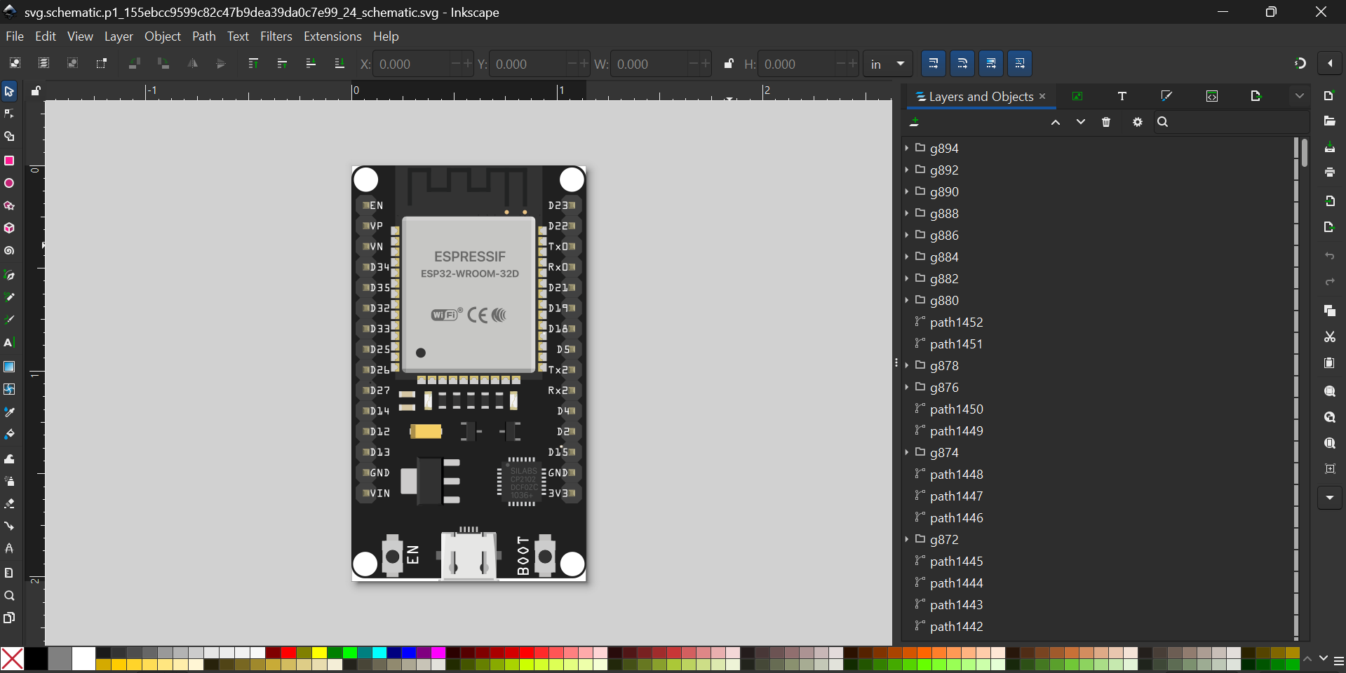
Ah! This part is indeed broken!
I couldn’t drag the part into the schematic or pcb views! Actually, the part has a few errors:
Schematic View
Schematic svg is wrong – it shows the breadboard image!
What I did to resolve the problem was to load Randy’s Inkscape Fritzing Schematic Extension and now looks fine.
PCB View
Same problem. Here is my edited PCB View:
@vanepp, can you please help me add in the layer id for breadboard view? It’s getting quite late at my side. Also, please check the attactched svgs (as I rushed through making them, and I may have made careless mistakes) and add in missing terminalIDs (if any). here’s my incomplete part.
NodeMCU-WROOM-ESP32_30pol-incomplete.fzpz (119.0 KB)
Thanks a lot!
OK here is a rather long check of your part with corrections. Starting with breadboard. There is a stray terminalId that can be deleted as it is expanding the viewbox which is undesirable.
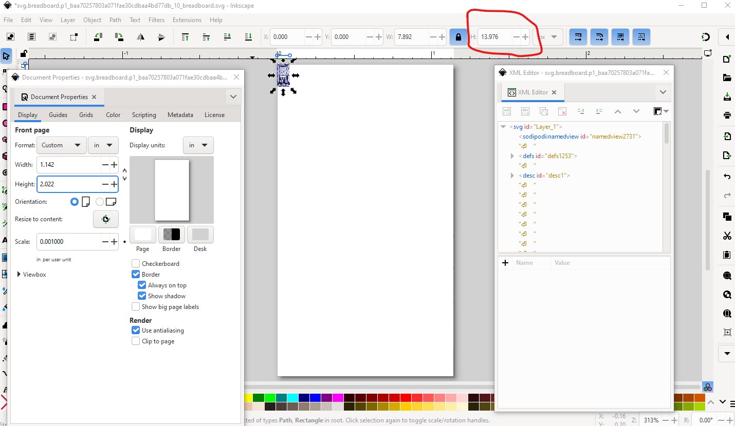
then the scale is incorrect (which won’t affect anything but is incorrect) so set up to rescale the image by ungrouping everything then setting the appropriate parameters for rescaling (as documented in the rescaling document)
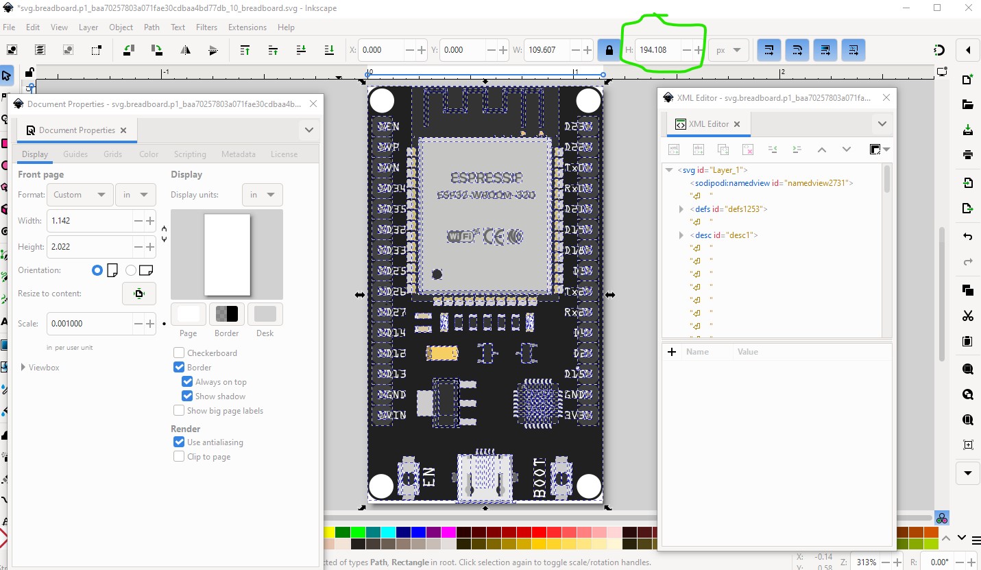
with dimensions set to px, copy the larger of the height or width (height in this case) to the clip board to set it after the rescale (which will change the size of the image like this)
now paste the saved height back in to the height parameter to restore the correct image size
to this
at the desirable scale.
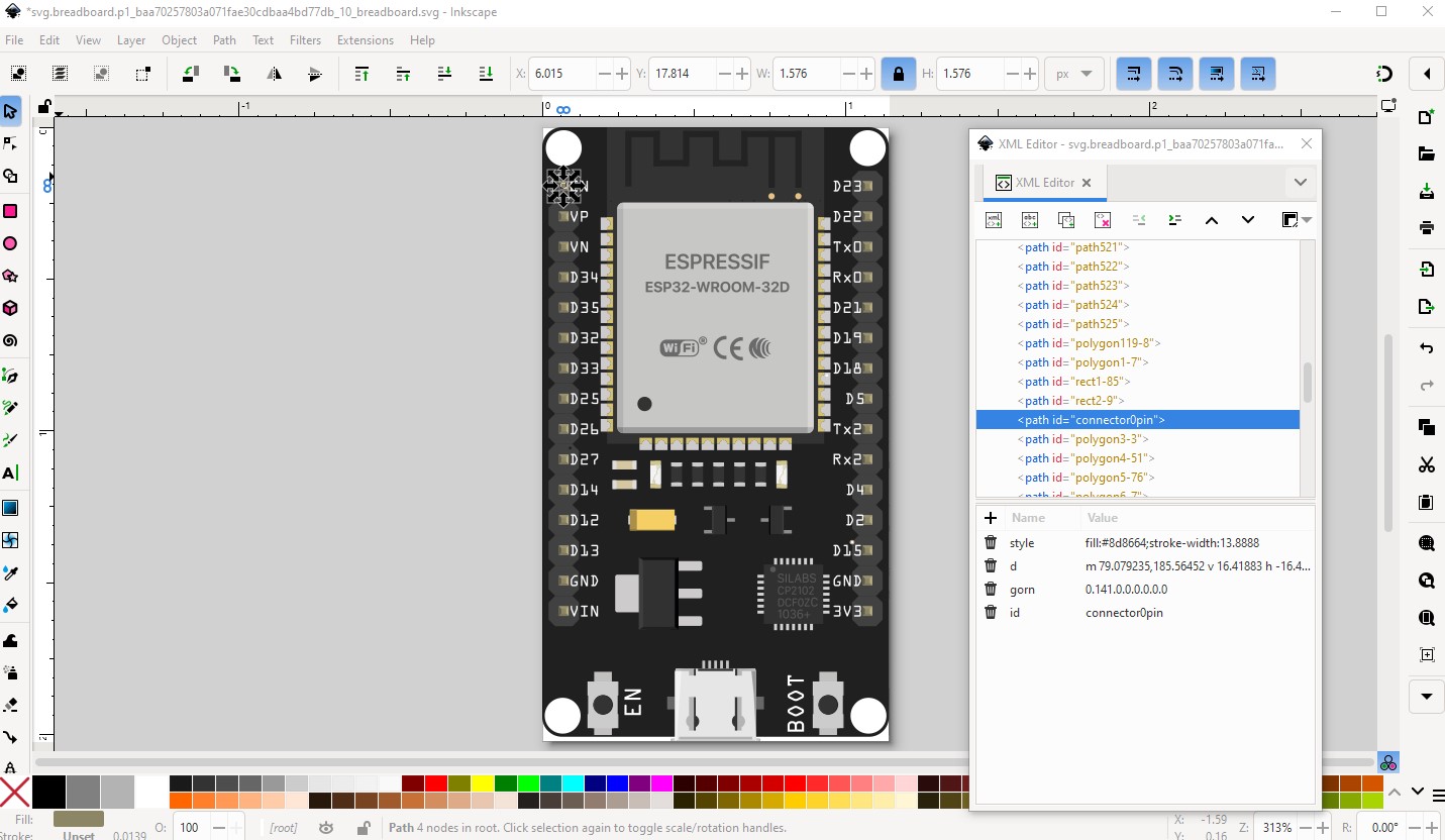
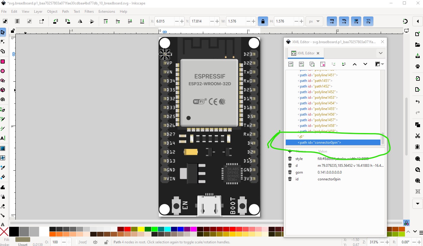
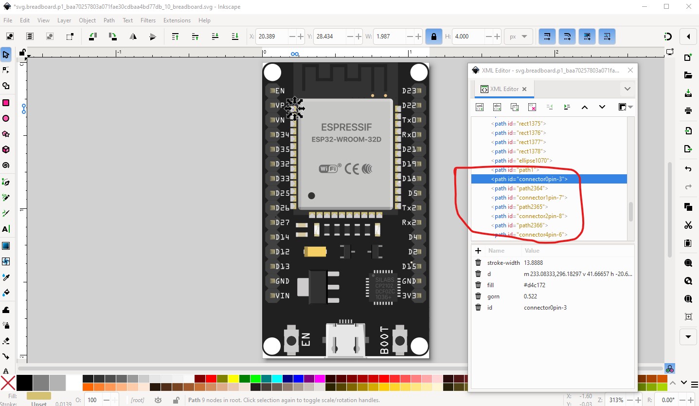
Now we need to move the connectors to the bottom of the svg in pin order (starting with connector0)
then we discover there are extra connectors (that likely aren’t in the fzp file and thus should be removed to reduce future confusion.) Since this is a common outcome in Eagle2Fritzing conversions I have a python script (currently not published) that fixes this.
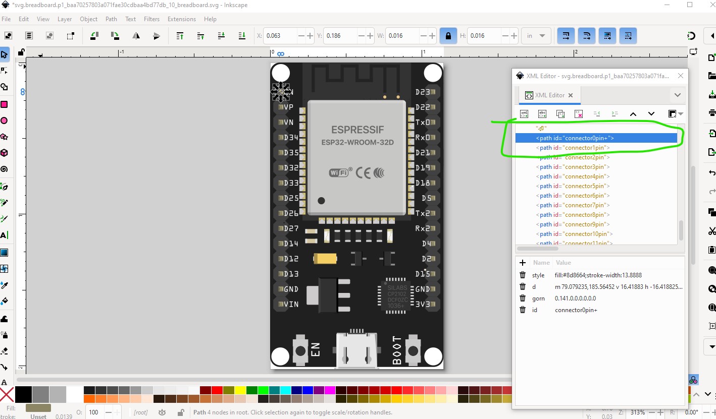
to do that I relabel connector0pin to connector0pin+ (which isn’t usually used in svgs) with the pins in order at the bottom of the svg
and then run E2fRemoveUnusedConnectors.py against the breadboard svg file like this:
$ E2fRemoveUnusedConnectors.py svg.breadboard.p1_baa70257803a071fae30cdbaa4bd77db_10_breadboard.svg
*** Process svg.breadboard.p1_baa70257803a071fae30cdbaa4bd77db_10_breadboard.svg ***
line 8646 connector ‘connector0pin-3’ deleted as unused.
line 8655 connector ‘connector1pin-7’ deleted as unused.
line 8664 connector ‘connector2pin-8’ deleted as unused.
line 8673 connector ‘connector4pin-6’ deleted as unused.
line 8682 connector ‘connector5pin-9’ deleted as unused.
line 8691 connector ‘connector6pin-7’ deleted as unused.
line 8696 connector ‘connector7pin-5’ deleted as unused.
line 8705 connector ‘connector8pin-4’ deleted as unused.
line 8714 connector ‘connector9pin-9’ deleted as unused.
line 8723 connector ‘connector10pin-2’ deleted as unused.
line 8732 connector ‘connector11pin-3’ deleted as unused.
line 8741 connector ‘connector12pin-1’ deleted as unused.
line 8750 connector ‘connector13pin-8’ deleted as unused.
line 8759 connector ‘connector14pin-3’ deleted as unused.
line 8768 connector ‘connector38pin-10’ deleted as unused.
line 8773 connector ‘connector38terminal’ deleted as unused.
line 8778 connector ‘connector39pin-9’ deleted as unused.
line 8783 connector ‘connector39terminal’ deleted as unused.
line 8788 connector ‘connector40pin-3’ deleted as unused.
line 8793 connector ‘connector40terminal’ deleted as unused.
line 8798 connector ‘connector41pin-3’ deleted as unused.
line 8803 connector ‘connector41terminal’ deleted as unused.
line 8808 connector ‘connector42pin-9’ deleted as unused.
line 8813 connector ‘connector42terminal’ deleted as unused.
line 8818 connector ‘connector43pin-5’ deleted as unused.
line 8823 connector ‘connector43terminal’ deleted as unused.
line 8828 connector ‘connector44pin-1’ deleted as unused.
line 8833 connector ‘connector44terminal’ deleted as unused.
line 8838 connector ‘connector45pin-5’ deleted as unused.
line 8843 connector ‘connector45terminal’ deleted as unused.
line 8848 connector ‘connector46pin-5’ deleted as unused.
line 8853 connector ‘connector46terminal’ deleted as unused.
line 8858 connector ‘connector47pin-2’ deleted as unused.
line 8863 connector ‘connector47terminal’ deleted as unused.
line 8868 connector ‘connector48pin-6’ deleted as unused.
line 8873 connector ‘connector48terminal’ deleted as unused.
line 8878 connector ‘connector49pin-0’ deleted as unused.
line 8883 connector ‘connector49terminal’ deleted as unused.
line 8888 connector ‘connector50pin-8’ deleted as unused.
line 8893 connector ‘connector50terminal’ deleted as unused.
line 8898 connector ‘connector51pin’ deleted as unused.
line 8903 connector ‘connector51terminal’ deleted as unused.
line 8908 connector ‘connector15pin-3’ deleted as unused.
line 8917 connector ‘connector16pin-3’ deleted as unused.
line 8926 connector ‘connector17pin-3’ deleted as unused.
line 8935 connector ‘connector18pin-1’ deleted as unused.
line 8944 connector ‘connector19pin-4’ deleted as unused.
line 8977 connector ‘connector36pin-7’ deleted as unused.
line 8982 connector ‘connector36terminal’ deleted as unused.
line 8987 connector ‘connector37pin-8’ deleted as unused.
line 8992 connector ‘connector37terminal’ deleted as unused.
line 9727 connector ‘connector0pin+’ changed to ‘connector0pin’.
line 9731 connector ‘connector1pin’ changed to ‘connector1pin’.
line 9735 connector ‘connector2pin’ changed to ‘connector2pin’.
line 9739 connector ‘connector3pin’ changed to ‘connector3pin’.
line 9743 connector ‘connector4pin’ changed to ‘connector4pin’.
line 9747 connector ‘connector5pin’ changed to ‘connector5pin’.
line 9751 connector ‘connector6pin’ changed to ‘connector6pin’.
line 9755 connector ‘connector7pin’ changed to ‘connector7pin’.
line 9759 connector ‘connector8pin’ changed to ‘connector8pin’.
line 9763 connector ‘connector9pin’ changed to ‘connector9pin’.
line 9767 connector ‘connector10pin’ changed to ‘connector10pin’.
line 9771 connector ‘connector11pin’ changed to ‘connector11pin’.
line 9775 connector ‘connector12pin’ changed to ‘connector12pin’.
line 9779 connector ‘connector13pin’ changed to ‘connector13pin’.
line 9783 connector ‘connector14pin’ changed to ‘connector14pin’.
line 9787 connector ‘connector15pin’ changed to ‘connector15pin’.
line 9791 connector ‘connector16pin’ changed to ‘connector16pin’.
line 9795 connector ‘connector17pin’ changed to ‘connector17pin’.
line 9799 connector ‘connector18pin’ changed to ‘connector18pin’.
line 9803 connector ‘connector19pin’ changed to ‘connector19pin’.
line 9807 connector ‘connector20pin’ changed to ‘connector20pin’.
line 9811 connector ‘connector21pin’ changed to ‘connector21pin’.
line 9815 connector ‘connector22pin’ changed to ‘connector22pin’.
line 9819 connector ‘connector23pin’ changed to ‘connector23pin’.
line 9823 connector ‘connector24pin’ changed to ‘connector24pin’.
line 9827 connector ‘connector25pin’ changed to ‘connector25pin’.
line 9831 connector ‘connector26pin’ changed to ‘connector26pin’.
line 9835 connector ‘connector27pin’ changed to ‘connector27pin’.
line 9839 connector ‘connector28pin’ changed to ‘connector28pin’.
line 9843 connector ‘connector29pin’ changed to ‘connector29pin’.
this has replaced the connectorxxx labels in the affected pins with something like circle1 (if the drawing element is a circle) so it is no longer labeled connector anything to avoid confusion with the real connectors. It also renumbers the connectors (which in this case were already correctly numbered) as it goes by. That results in this
with the only connectors being the ones in use at the bottom of the svg. Then do an Edit->select all and Object->group and rename the group to breadboard to form the breadboard layerId
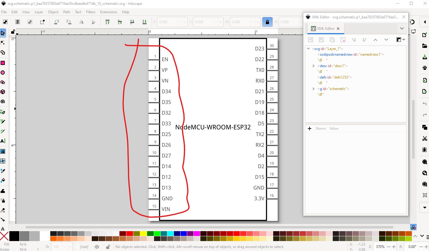
then save the resulting svg as a plain svg as breadboard is no complete. So on to schematic (only minor problems here!)
the pins on the left should move up one position so they match the ones on the other side (the height in the schematic extension was 0.1in to large and it sometimes gets the pin order offset by 1 in that case) so ungroup the svg and correct that. Select all the pins on the left and (with dimensions set to inches!) click the y decrement icon to move them up 0.1in
then select the rectangle and decrement the height by 0.1in
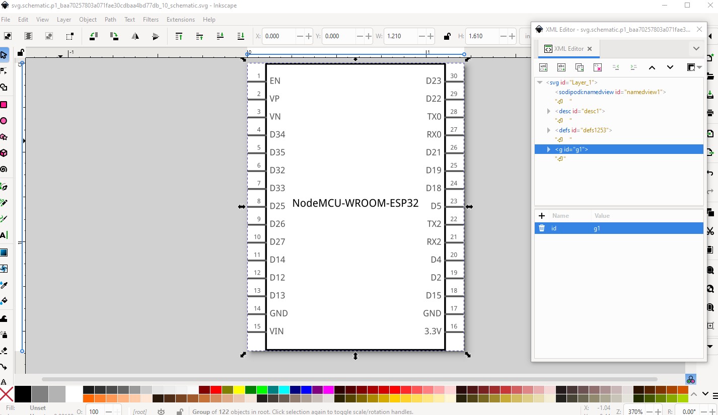
then Edit->select all, Edit->resize page to selection to reset the viewbox then Object->group and set schematic as the layerId and save the svg as completed.
then on to the pcb svg.
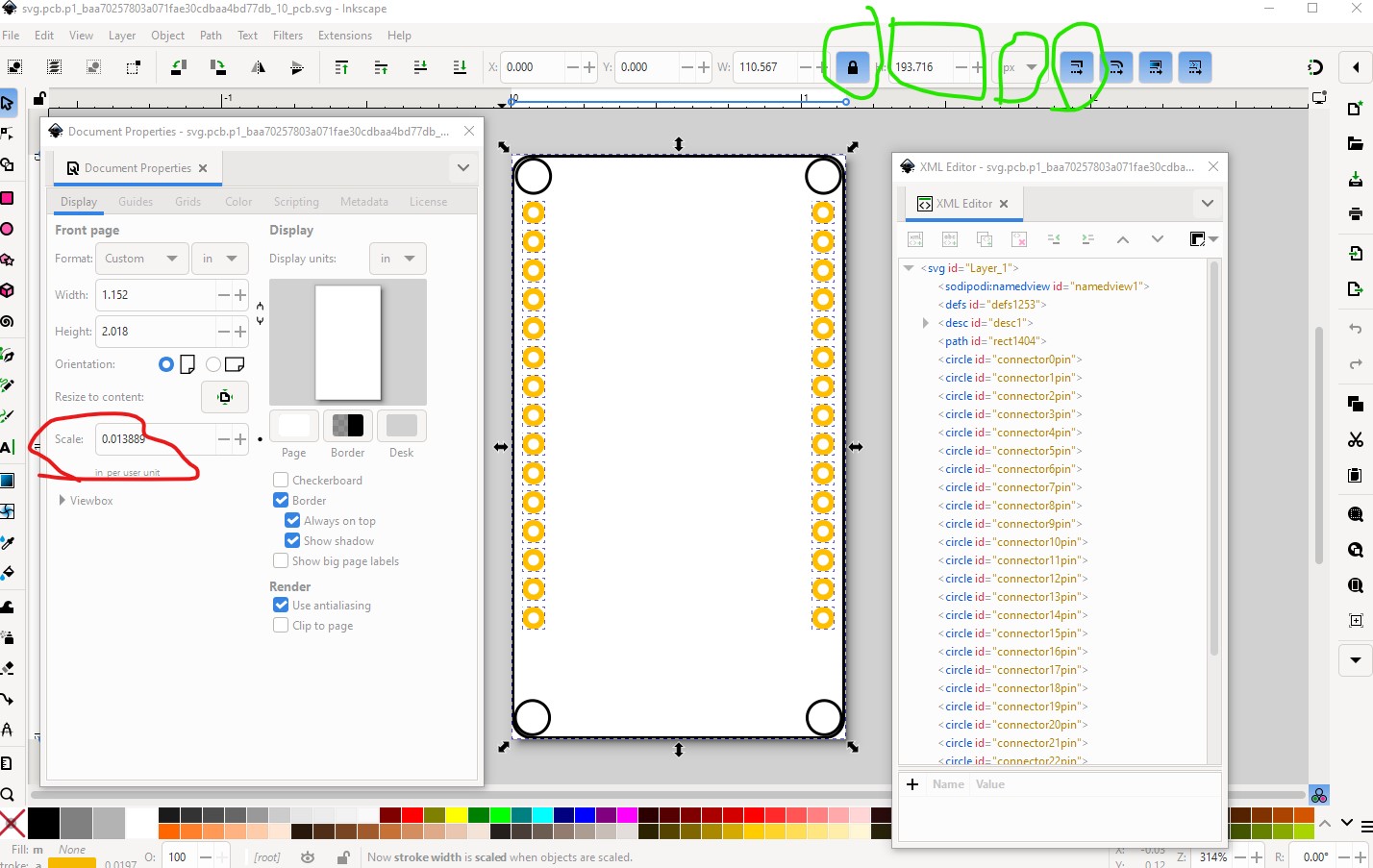
again the scale isn’t correct (and the correct scale makes other stuff easier to see!) so rescale it
first do an Edit->select all, then object group to group the entire svg in a single group
then select the new group and press the alt-cntrl-g (ungroup) key multiple times to ungroup the entire svg so it can be rescaled (rescaling with groups in place will cause transforms which is undesireable!)
with that done we see the connectors are not in order at the bottom of the svg, so first correct that.
then rescale the svg to the correct scale saving the height as the larger of height and width first
then restore the height to resize the image
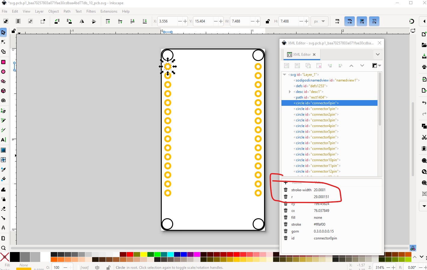
now we are at the correct scale, we check the pads to see they are the correct size. For a 0.1in header that should be 0.038in which at this scale is a radius of 29 with a stroke-width of 20. As we see the pads are slightly missized at stroke-width 20…001 and radius 29.000151 (probably due to floating point roundoff in Inkscape!) while I could manually do this for each pin in Inkscape the lazy method (which I always choose!) is to save the svg, then edit it in a text editor (I use vi) and do a global replace to set the stroke-width to 20 and the radius to 29
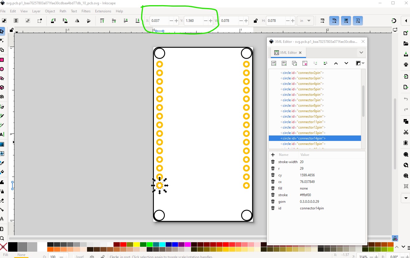
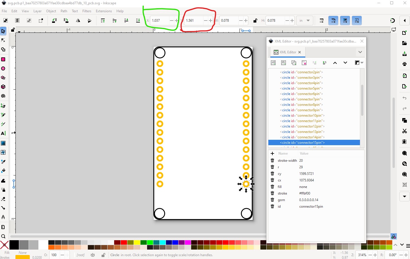
next because this is someone else’s svg, it is a good bet to check the pin spacings are correct. In this case the left pins are fine, they are all on exactly 0.1in boundaries as they should be, but the pins on the right are 0.001 to far right. While 1/1000 of an inch makes no practical difference I prefer to have the dimensions accurate
the y coords are all 0.001in lower than the right, so select them all and move them up 0.001in
so they align exactly.
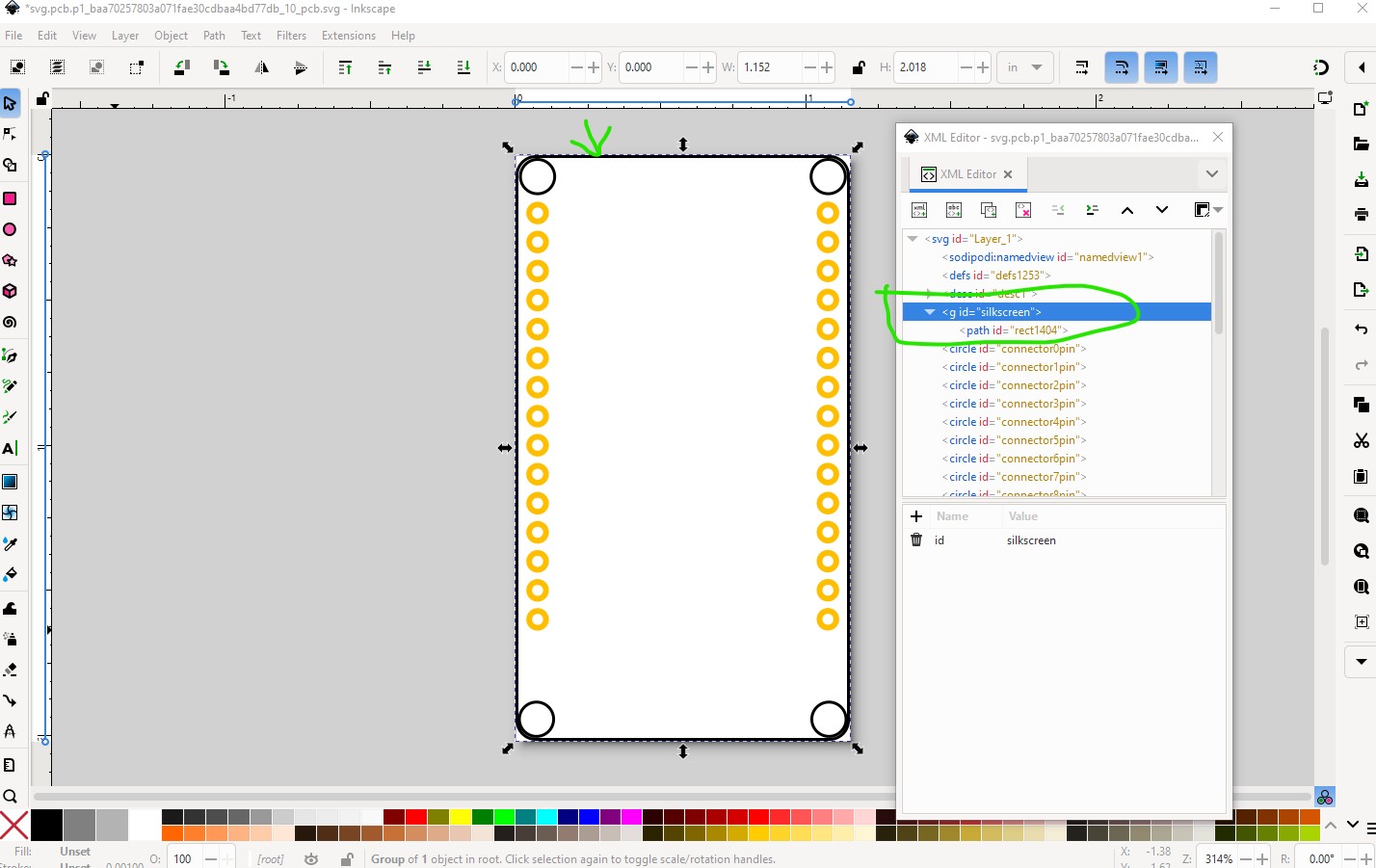
Now add the necessary groups, starting with silkscreen, so select the silkscreen path and group it and set the label to silkscreen
then do the same (except with 2 groups) for the connectors
then save the pcb svg as completed. Now on to the fzp file. First thing to check is that the buses are correctly configured. This is a common error as people making parts don’t necessarily know about buses and may have a configuration for the original part (which is now wrong) and didn’t know to change it. In this case the bus definition is correct, only the 2 ground pins are in a bus as they should be
 <buses>
  <bus id="GND">
   <nodeMember connectorId="connector13"/>
   <nodeMember connectorId="connector16"/>
  </bus>
 </buses>
(I did change the bus name from Internalbus1 to GND to better describe what the bus is but either would do.) With that things should be correct so run FritzingCheckPart.py against the part to make sure all is well:
$ FritzingCheckPartw.py part.p1_baa70257803a071fae30cdbaa4bd77db_10.fzp
**** Starting to process file Startup, no file yet
…(warning removed to save space)
Error 18: File
‘part.p1_baa70257803a071fae30cdbaa4bd77db_10.fzp.bak’
Connector connector1terminal is in the fzp file but not the svg file. (typo?)
svg svg.breadboard.p1_baa70257803a071fae30cdbaa4bd77db_10_breadboard.svg.bak
Error 18: File
‘part.p1_baa70257803a071fae30cdbaa4bd77db_10.fzp.bak’
Connector connector4terminal is in the fzp file but not the svg file. (typo?)
svg svg.breadboard.p1_baa70257803a071fae30cdbaa4bd77db_10_breadboard.svg.bak
while this is flagged as an error, because it is breadboard it isn’t actually an error and would be ignored if left alone as the terminalId is no longer defined in the svg file, but to be correct I edited the fzp file to remove the breadboard terminalIds like this
    <connector id="connector1" name="VP" type="male">
      <description>pin 2</description>
      <views>
        <breadboardView>
          <p layer="breadboard" svgId="connector1pin" terminalId="connector1terminal"/>
        </breadboardView>
to
    <connector id="connector1" name="VP" type="male">
      <description>pin 2</description>
      <views>
        <breadboardView>
          <p layer="breadboard" svgId="connector1pin" />
        </breadboardView>
Then FritzingCheckPart.py runs without complaints
$ FritzingCheckPartw.py part.p1_baa70257803a071fae30cdbaa4bd77db_10.fzp
**** Starting to process file Startup, no file yet
**** Starting to process file part.p1_baa70257803a071fae30cdbaa4bd77db_10.fzp
**** Starting to process file svg.breadboard.p1_baa70257803a071fae30cdbaa4bd77db_10_breadboard.svg.bak
**** Starting to process file svg.schematic.p1_baa70257803a071fae30cdbaa4bd77db_10_schematic.svg.bak
**** Starting to process file svg.pcb.p1_baa70257803a071fae30cdbaa4bd77db_10_pcb.svg.bak
File
‘part.p1_baa70257803a071fae30cdbaa4bd77db_10.fzp.bak’
This is a through hole part as both copper0 and copper1 views are present.
If you wanted a smd part remove the copper0 definition from line 43
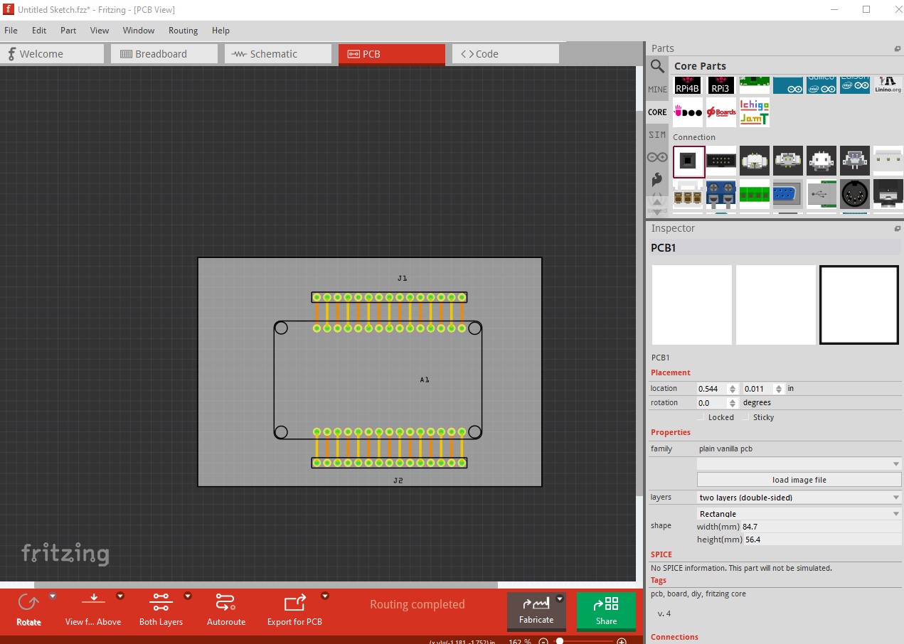
so the part should be complete so make it back in to a part
NodeMCU-WROOM-ESP32_30pol-fixed.fzpz (52.7 KB)
and test it
which all looks OK so export it as gebers and check it in gerbv for correctness (as gerber processing happens after pcb rendering errors can appear in the gerber output that don’t in Fritzing.)
checking all the expect holes are present is the first thing to check (this has the top copper layer suppressed to make the holes more visable.) As that all looks OK, check the drill.txt file (Untitled Sketch_drill.txt in this case) to make sure the hole sizes are correct
; NON-PLATED HOLES START AT T1
; THROUGH (PLATED) HOLES START AT T100
M48
INCH
T100C0.038000
%
T100
X025555Y015333
which they are the line
T100C0.038000
indicates all the hole are 0.038in as they should be for 0.1in headers. So the part above should do what we want.
Peter
Thanks for your effort. Incredible, but way too complicated for me.
I think EasyDA is more suitable for me.
But, thanks again!