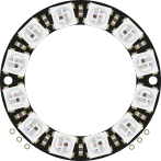
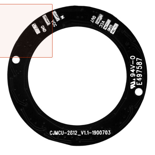
I bought this module, but I can’t create or find the part for the AZ Delivery LED ring RGB 37mm. The connection pins don’t exist — they are surface pads, so through-hole pins would be needed, as shown in the attached documentation.
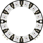
Name of the part: AZ Delivery LED ring 5V RGB WS2812B 12-bit 37mm
Type
I did not read this
Breakout board, sub assembly, plug in module (A)
Antenna (AE)
Battery (BT)
Capacitor (C)
Diode (D)
Display (DS)
Fuse (F)
Hardware , mounting screws, etc. (H)
Jack, fixed part of a connector pair, header (J)
Relay (K)
Inductor, Coil, Ferrite bead (L)
Loudspeaker, Buzzer (LS)
Motor (M)
Microphone (MK)
Plug, moveable part of a connector pair (P)
Transistor (Q)
Resistor (R)
Thermistor (RT)
Varistor (RV)
Switch (S)
Transformer (T)
Integrated Circuit (IC)
Crystal, Oscillator (Y)
Zener diode (Z)
Other (surface mount component but with round through-hole pads for wires)
Yes indeed, I hadn’t thought of reusing the Adafruit module. In terms of dimensions, the AZ Delivery one is 37mm with 7mm LEDs, just like the Adafruit module actually. The only differences are the connections not being in the right places, and the mounting holes also need to be added. But yes, it does match well.
In short, comparing the two modules:
Adafruit 4 pins: GND/5V/IN/OUT
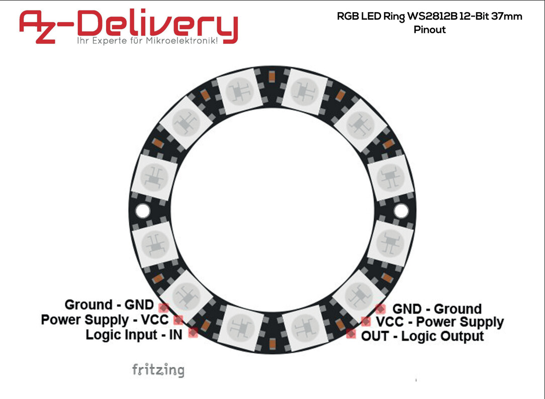
AZ Delivery: 3 pins on one side: GND/5V/IN and on the other GND/5V/OUT. To tap the power supply for daisy-chaining.
Thanks for your quick reply.
Hello. I haven’t read your message in full, but yes, the file that is not to scale does indeed have 6 connectors. On the AZDelivery, these are tinned traces on the component, which is why the 6 connectors were added on the outside so that the wires can be soldered onto the PCB, and on the surface of the component. I’ll grant you that, it’s not straightforward. Here is a view of the back of the LED ring:
I’ve gone ahead and adjusted the breadboard file first.
I’ve brought it to the dimensions of 37 mm. I hope that matches the original.
I’ve also renamed the 6 connectors and moved them to the very end of the file, and I’ve renamed all objects that started with connector. I did all of this in the XML editor with Inkscape.
Now, regarding the PCB view — does it only have SMD pads and no THT contacts (holes)?
You can’t really solder those onto a circuit board at all, can you?
I could try placing THT contacts (solder holes) as a footprint where the solder pads currently are.
Is the ring actually meant to be soldered onto a circuit board?
If not, we’ve got it easy. If so, we’ll need to work very precisely.
Super job, it imports perfectly, thank you. As for the ring, I don’t want it soldered directly, hence the addition of the 6 “pads” at the bottom on either side of the ring, so it’s a “floating” component that will be on a PCB but connected via “flying” wires. On the breadboard view, I placed them opposite the SMD solder points, they can be aligned if needed. There will just be a few more wires to add anyway thank you very much for your work,
so for my setup I indeed only need 3, but if I want to chain multiple rings, all 4 are needed because three for the input, and three for the output
Left side Vin/GND/IN
Right side VIN/GND/Out for chaining without having to go back to the starting point.
let’s keep it simple, anyway on a daisy chain on a printed circuit board, there’s no need for it. So ok for 4 pins in the form of a header with VCC GND IN OUT. That does simplify everything indeed.
In the meantime, I received the rings, despite the “sparse” documentation, the outer diameter is not 37 mm but 39 mm. So there might be a small scaling adjustment needed. I tried last night, I installed Inkscape, and I have to admit I’m struggling a bit with it — even though it’s as user-friendly as Illustrator, I don’t have the “right” reference points, and as a result I can’t yet figure out how to simply increase the “work area”, if I can call it that.
In any case, thank you for your valuable help.
Kind regards.
Ok, for the schematic view, it might indeed be more sensible to include all 6 pins and use internal connections.
For the PCB view, 4 pins are enough, and — maybe I’m asking too much — but would it be possible in the PCB view to have the silkscreen of the ring with the drill holes, but just as silkscreen? So that we can see where the holes will need to be drilled and therefore avoid placing traces where the holes will be
 : AZ Delivery LED ring 5V RGB WS2812B 12-bit 37mm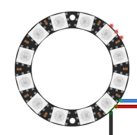
 anyway thank you very much for your work,