I followed the tutorial to draw a custom pcb with cutouts. Fritzing loads the custom svg and displays the cutouts properly. But when I export to gerber files, the cutouts seem to be vanished.
Thanks for your help.
DH
I followed the tutorial to draw a custom pcb with cutouts. Fritzing loads the custom svg and displays the cutouts properly. But when I export to gerber files, the cutouts seem to be vanished.
Thanks for your help.
DH
PCB’s are fairly easy to make with cutouts and unique shapes. But, it is not straight forward without a bit of help.
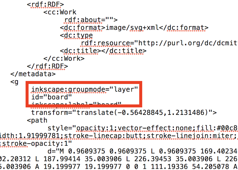
Creating an SVG and loading it is simple but, it’s the details in the XML file that enable Loading and Exporting with desired results.
There are many Guidance posts and tutorials so I won’t repeat them here. Rather, knowing that organizing and planning ahead, along with usage of Inkscape and it’s XML editor-panel are the answer. Yes, you can use other Drawing app’s as well.
You can open a simple PCB example SVG (from Fritzing) in a Text Editor (the XML is Text and will load so you can inspect and edit it per the Help/Instructions you find).
And, it can be fussy, very fussy, particular about syntax/details.
In the end, you’ll end up with an SVG having Layer label’s (like ‘board’, ‘silkscreen’, …etc) that inform Fritzing of what to do with the elements.
Example is provided. Note: For Exporting success, I added two parts (LED & Resistor) to avoid Error Msg…
Screenshot of portion of XML, PCB. The PCB example file attached…
Screenshot of the Gerber output (of Contour)
Good luck,
PCB_Example.fzz (2.6 KB)