This may help…
Quick (5 minute) read to understand the elements of pcb/silk/mask Not important to understand his use of software he’s using, just understand the elements of Silkscreen, Soldermask, etc…
Example of custom graphic for the Silkscreen of a Part (could be for a part, a section or cover the entire board).
Also, the board itself (apart from the “Part’s” on it, which includes adding silk as indicated above) can have it’s own silkscreen that gets loaded by adding your own pcb shape. Attached (delete the fzp extension) pcb.svg.fzp (126.9 KB)
(in otherwords, can have a Silkscreen on the board implemented as a Part graphic or, implemented as part of the PCB’s shape.)
Example of a pcb to be loaded in place of the default pcb (via using the Inspector to load it). It also contains a Cutout
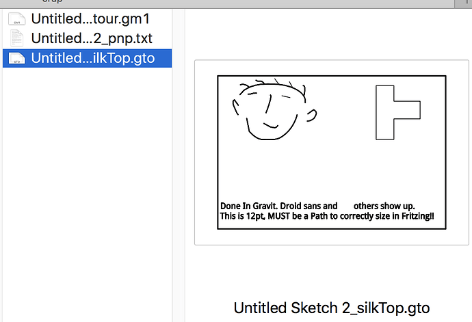
Also shows is Gerber of the silk layer
