Custom Soldermask In Parts & Some begginer stuff

Hi all =]’

I’ve being Investigating FZ features for some time in order to learn how to create some artistic boards I have in mind and I stuck upon some annoying issue: I’d like to create custom soldermask that doesn’t necessarily related to other features of a part like copper connections placement and, for the life of me, couldn’t get it to work.

Let’s get technical:
This picture ( https ://imgur.com/a/JR6j3ZJ ) shows a regular image on PCB using the built-in part that lets you pick a picture and it’ll make it onto the PCB’s copper layer. Note that most of the Iron Man there is covered in soldermask. To the left you can see a part used as soldermask remover (after nights of digging the web and the forums on how to remove soldermask and countless attempts and edits to SVG files) that removes the whole soldermask effect from the area in question.

The problem is that it is two different parts and therefore needs alignment and some other small problems arise.
Since this problem rose from a artistic demand, my ultimate favorable workflow would be something like this: working on some picture in AI, setting up the layers conveniently for FZ then creating a single part that will include complex copper and soldermask areas placement.

I will note before I ask my questions that I viewed almost every available YouTube video I could lay my hands on and couldn’t find the answers, the forums were a lot more helpful but still couldn’t make it to the final stretch.

Since I’ve seen some advanced people around here knowing deeply how FZ works and analyzes the SVG’s we feed into him, here’s my questions:

1.) What layers does FZ actually process? what is the structure of the SVG should be like?
here’s a picture of an example SVG for PCB tab/layer/section found on FZ website as instructional material ( https://imgur.com/a/EXRuxJp ) - after opening several hundreds of part files submitted by the community, still haven’t seen dominant layer structure or grouping order. Some file had the copper1 layer inside 20-layer cascaded groups, some had none. No matter what I did in the ‘soldermask’ layer, it didn’t have any seen effect in FZ or Gerber exports.

2.) I’d like to know which tags inside the SVG file is relevant to FZ and what they does. In this picture ( https://imgur.com/a/8LKNi6r ) you can an example file opened in Sublime and I don’t know what all the tags mean in the start of the file. For example, I did notice that I need to add " fill-rule=“evenodd” clip-rule=“evenodd” " to parts that I created to use as soldermask remover.

3.) I’ve notice that if the order of the layers is different, there are variations in the results after importing to FZ Parts Editor, for example if copper0 & copper1 is switched, it messes with the top layer in one case and not in the other, so- Is there any particular order all the various layers should be at?

I know I came in here and for my first post I’ve bombarded you with questions but I really desperate after all the digging…I’ve wanted to add files to prove my various points but since I’ve done hundreds of tests and Gerber exports very fast while I was working on it, it is very hard right to find specific files so if you guys would ask for files about specific incident, I will generate new files for your questions and post them for you to see.

Thank you so much, everyone!
Kimkash
This may help…

Quick (5 minute) read to understand the elements of pcb/silk/mask Not important to understand his use of software he’s using, just understand the elements of Silkscreen, Soldermask, etc…

Example of custom graphic for the Silkscreen of a Part (could be for a part, a section or cover the entire board).

Also, the board itself (apart from the “Part’s” on it, which includes adding silk as indicated above) can have it’s own silkscreen that gets loaded by adding your own pcb shape. Attached (delete the fzp extension) pcb.svg.fzp (126.9 KB)

(in otherwords, can have a Silkscreen on the board implemented as a Part graphic or, implemented as part of the PCB’s shape.)

Example of a pcb to be loaded in place of the default pcb (via using the Inspector to load it). It also contains a Cutout

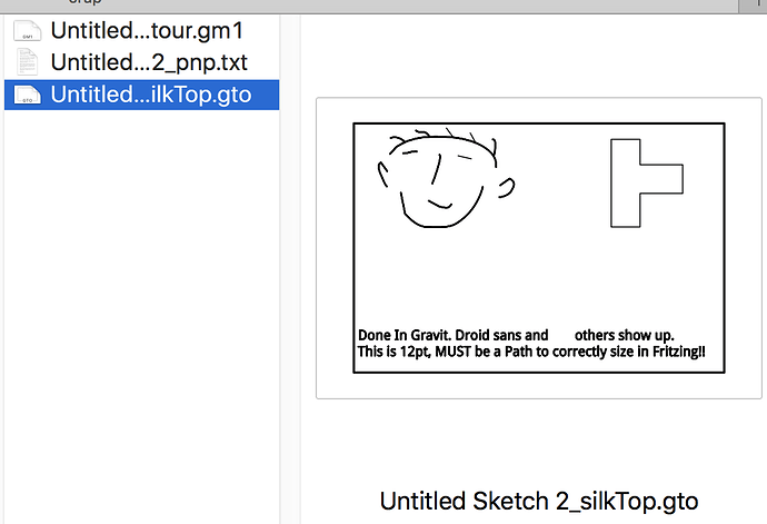
Also shows is Gerber of the silk layer

pcb

I don’t believe you can make that work directly. The solder mask AFAIK is not a layer, it is generated from the copper portions of a part. That has been done (but I don’t think will work in your case) is to generate a part that has the solder mask you desire, keep a copy of the gerber mask file, then redo whatever you removed that generates an incorrect mask, and convert to gerbers, then substitute the original gerber mask file in to the gerbers to generate the effect you want. If you can figure out how to generate a gerber mask file with the design you want that should work. Something else that may work for you is so called “invisible copper” (which is actually likely a bug). If in a copper layer (which ever one you want the mask for, copper0 for bottom, copper1 for top) you can block mask by setting the fill on a copper element to none rather than the usual copper color. That will block mask on the area coverd by the invisible copper. You however can’t add mask to anywhere that has copper, only remove it leaving bare board instead of copper. This is a limitation of how Fritzing generates masks.

This dosen’t resolve as a url so I can’t see the image. The text after that indicates you may already have found invisible copper though.

Depends on what is defined in the fzp file, and what Fritzing supports. The typical ones are these (there may be more I haven’t run across though):

breadboard
icon
pcb
silkscreen
copper1
copper0 (as a child of copper1)
(contour, silkscreen0 and possible others optionally)
schematic

In this configuration it is important that any translates in the copper layers either be removed or identical in both layers (otherwise the changing a component from top to bottom of the board breaks). Groups (other than the group names of layers that occur in the fzp file) are irrelevant, the parts editor loves to create unneeded groups (possibly for some valid internal reason I don’t know), but does’t care if you remove them all (as I usually do). Most of the time so is layer order, although the preferred order of pcb runs to

silkscreen
copper1
copper0 (child of copper1)

silkscreen at the top because that affects selection (with silkscreen on the bottom, in pcb view it prefers to select silkscreen which is rarely what you want), but the other orders will usually work sometimes with some changes. Fritzing tries to be flexible and tolerant. There are also case (mainly compatibility with old parts but other reasons as well) where this layout is useful (but causes problems with Inkscape on through hole parts)

silkscreen
copper1
copper0

Parts editor does not support this format though and for a through hole pad you need the identical pad including the same id on both copper0 and copper1 and Inkscape at least does not support that. This configuration allows you to put traces between connectors in a part (with some manual effort). With the copper0 a child of copper1 setup all traces will appear on both layers which makes running traces difficult.

Interesting, that is the first instance I’ve seen where either of those had an effect in Fritzing. They are usually added by the svg editor (Inkscape in my case) for reasons of its own and I usually remove them. Other than that, there is no documentation that I am aware of (other than the source code) for what tags are used. I know that some parts of Fritzing (bendable legs in particular) don’t support style commands and thus you need to convert them to inline xml instead. Gerber processing does not support inheritance so you need to make sure there is a stroke-width (inherited from above if necessary) present in the circle definition in the pcb copper layer along with a radius (not an ellipse) in order for the gerber code to generate a hole in the pcb. There are probably more that I haven’t run across (or have forgottein :slight_smile: ) as well.

Peter