So I’m trying to make a custom part for a a very specific need. The problem I’m having is I need part of it to NOT have the solder mask on. I want it to be the pcb uncovered.
No matter how I edit my SVG as soon as I add a wire I get an error
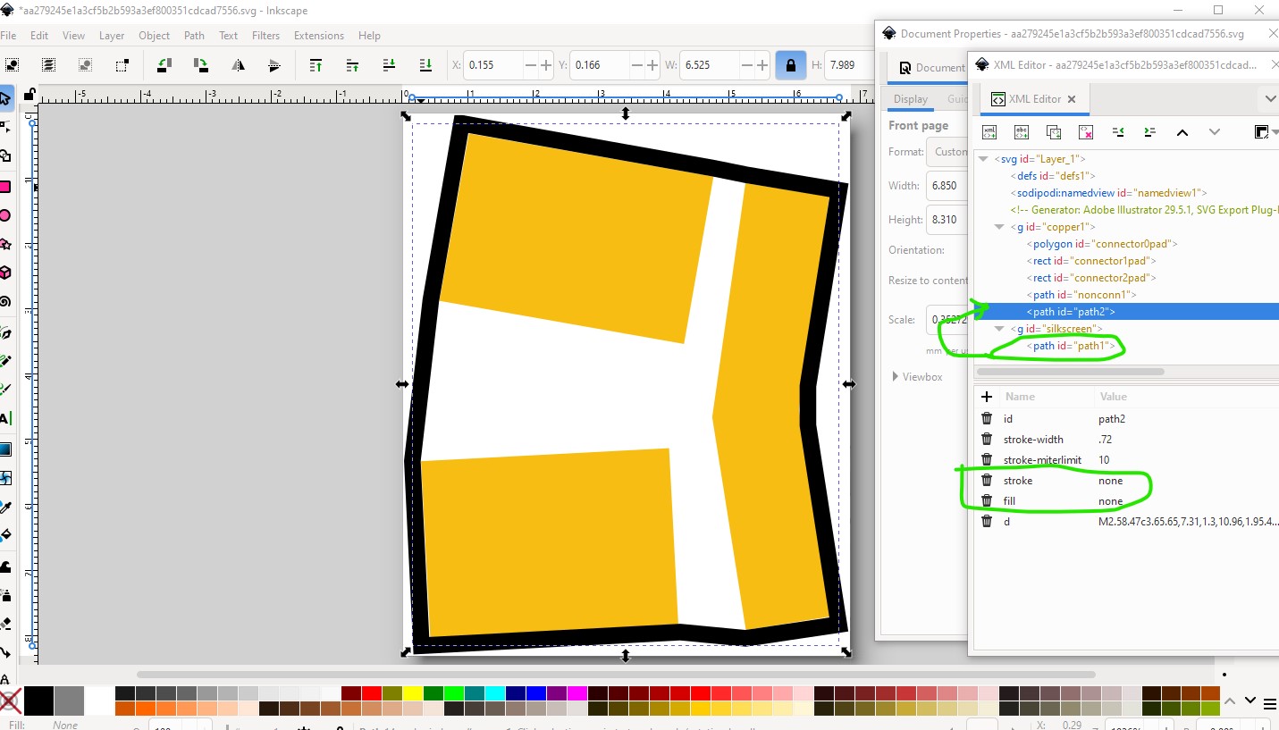
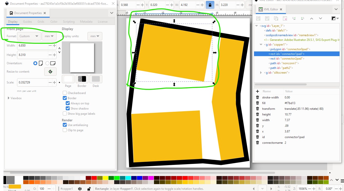
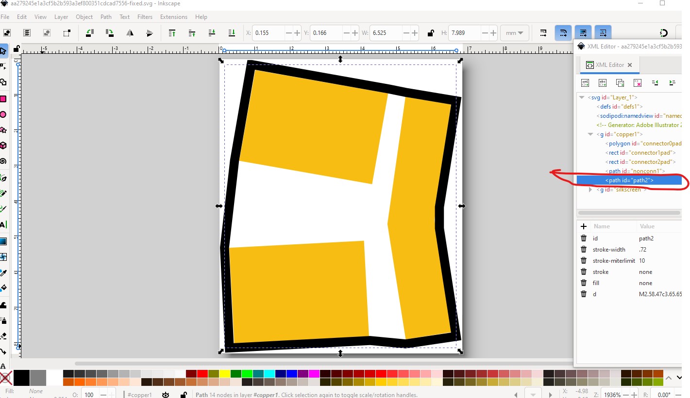
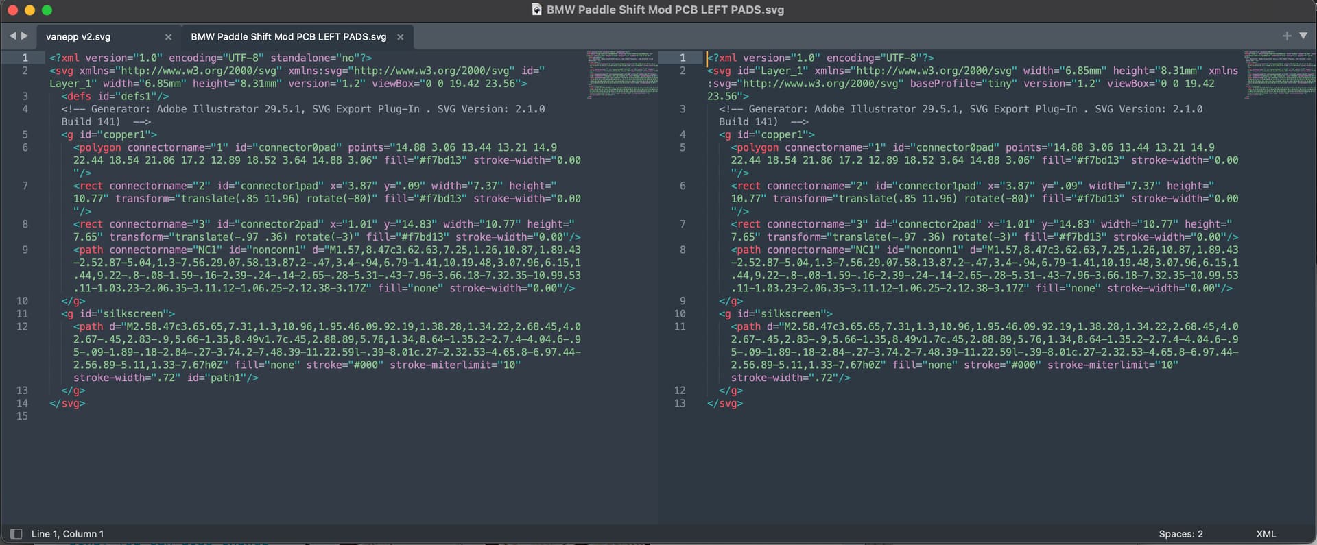
The path needs to be in the copper layers not silkscreen and have no stroke nor fill. This svg should do what you need:
It looks like this with the path in silkscreen duplicated and moved to the copper layers and the stroke set to none (so it doesn’t produce copper.) that will block the mask without adding copper (although check it with a gerber viewer to make sure as I don’t have a part to try it on handy.)
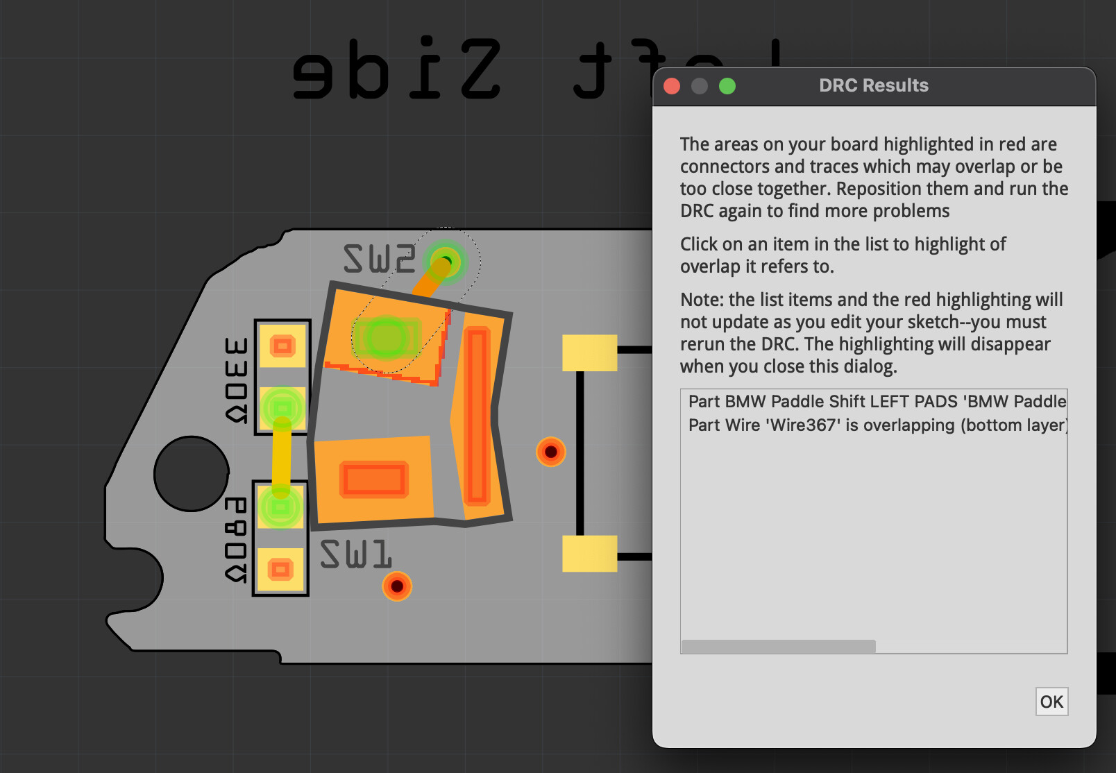
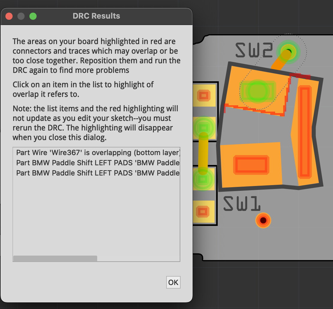
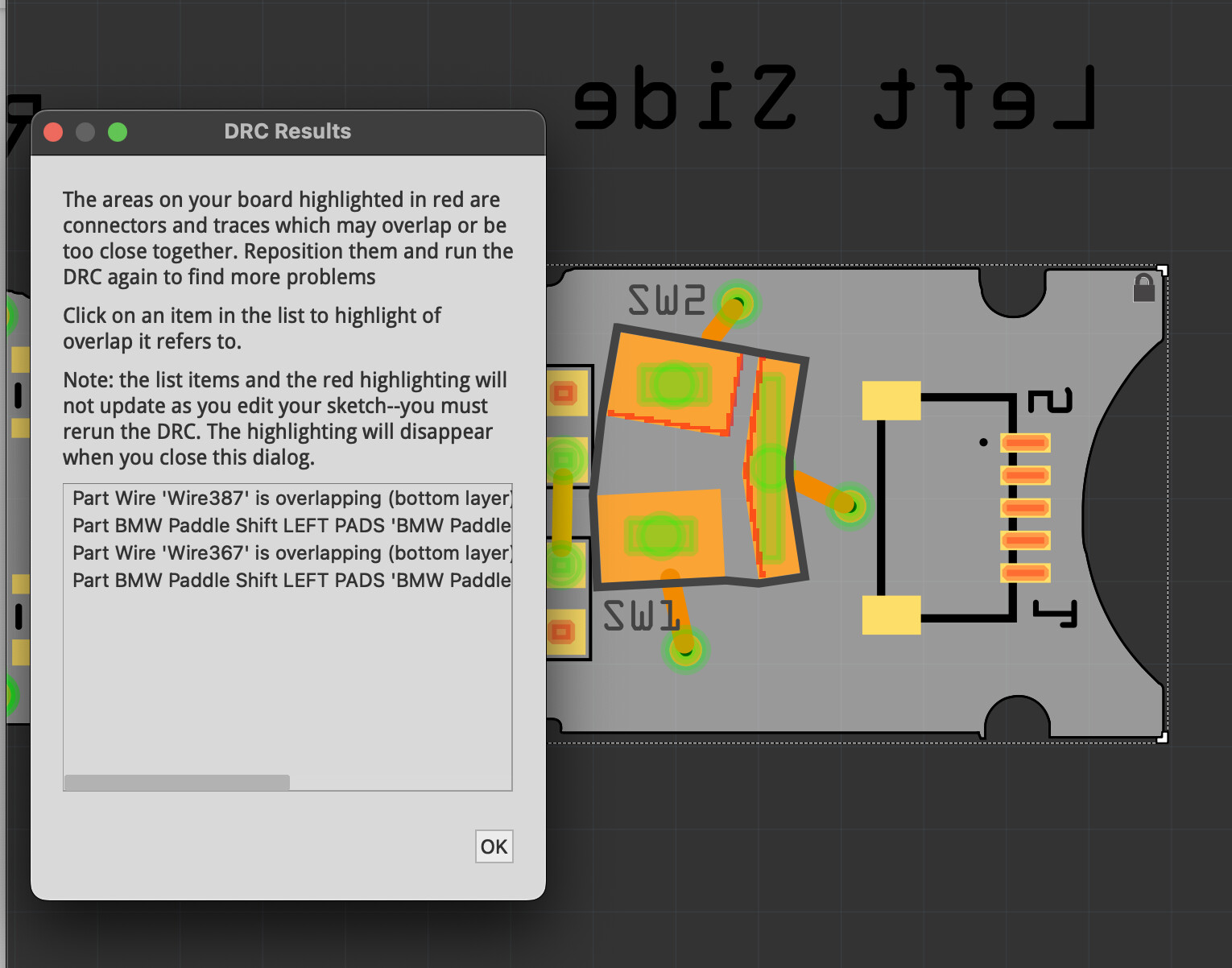
There shouldn’t be DRC errors although it may be a bounding box issue, as the bounding boxes overlap (although that doesn’t match what DRC is reporting either)
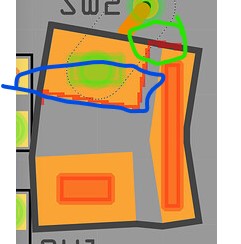
the overlap (if DRC uses the bounding box, which I don’t know that it does, it may calculate the actual path separation, I don’t know enough about DRC processing to say) do overlap. It should be ignorable as the copper looks right though (a gerber viewer is the best way to tell that.) The red from the DRC report should only be in the area circled in red (I think!) not the entire side circled in blue which doesn’t appear to be in conflict.
Incidentally, this svg is dimensioned correctly in mm rather than px.
I expect that will work fine. I don’t exactly know what is upsetting DRC in this. I would expect it to complain about the bottom copper too but it isn’t. There isn’t anything in the svg that I can see (except the mask rectangle) that should cause a problem. The mask rectangle is utilizing a bug in 0.9.3b (where it was created) that may have been fixed in later versions (I haven’t used it much and I don’t think in any of the later versions) You will want to check the gerber mask layers to make sure the mask has indeed been suppressed but I think this still works…
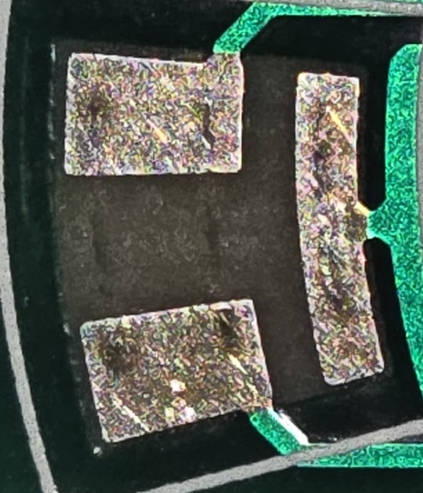
I did do a gerber test earlier (albeit no wires attached to part) and the solder mask / no solder mask area showed correctly as expected. Ill will check it again once ive completed my design
Unless it has changed in recent versions, DRC actually works from zoomed in pixels. It renders the copper, then expands one piece at a time by the configured separation distance, checking for overlap with other rendered copper. I had occasion to dig into that piece of code some years ago. At a glance, there must be 2 separate pieces of copper there, that Fritzing is thinking are separate nodes. If they are not really separate, ignoring the warning is fine.
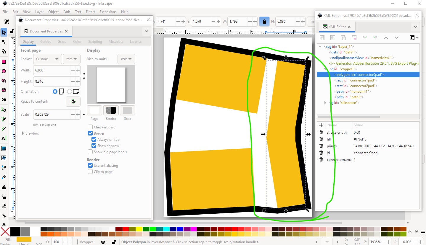
@microMerlin I am at fault. I didn’t see the existing invisible copper and added another one which will likely be causing the overlap. This is the original correct one:
which overlaps with the one that I added although they are both invisible because of stroke=none and fill=none. That is likely what is causing the overlap which should go away with this svg.
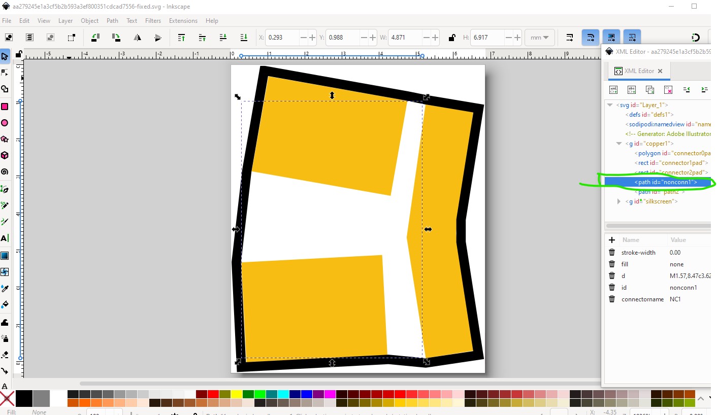
which only has the original invisible copper. @IAmOrion try this one and see if DRC indeed becomes happy (I expect it should.) The placement of the red lines is odd because that is in the middle of the overlap but the invisible copper may confuse DRC.
Unless I’m being dumb, the one uploaded in your last post - included above, is almost identical to the original file I uploaded with the exception of id="path1" added on the silkscreen?
EDIT: Still generates DRC error - It has to be because of the “invisible” (no fill) copper bit in the middle. For whatever reason, DRC does not like it once a wire is connected. With nothing connected, it passes DRC fine.
I agree! I’m OCD so normally like the DRC to pass and have zero issues, but I think on this very rare occasion, any DRC errors regarding that particular part I will have to ignore and obv check in gerber viewer before paying to produce
To get DRC happy, you would need to somehow get that extra copper to be in the same ‘net’ as the wire you connect. Then it will know that the overlap is fine. It needs to be (part of) a ‘connector’ and get attached to the net.
I expect the problem there is that it likely spans more than one net which will cause an overlap. So just ignoring the DRC error may be the easiest solution.
I wanted to update this post to say I went ahead and had the PCB created by JLCPCB. Turned out perfect despite the DRC errors. Works perfectly as expected, so on this occasion, ignoring DRC errors specifically to that part was fine and all worked out! Thanks to all and especially @vanepp for their help