Custom part, opposite pads

Hi,

While trying to create a custom part, I ran into an issue. At this point I’m not sure if this is a bug or something I am doing wrong…

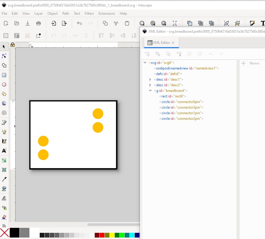
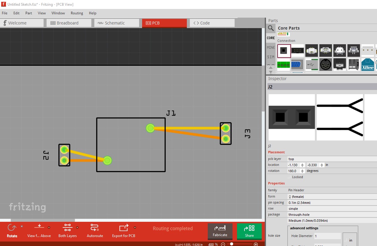
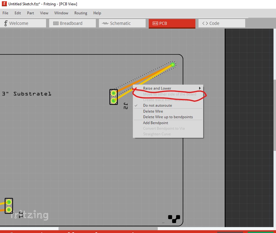
The part has a PCB and on both sides it has two pads. Although the pads are exactly in the same X/Y position on both sides, they are not via’s (top and bottom not connected):

The pads on the top layer (copper 1) have id’s 0 and 1. The pads on the bottom layer (copper 0) have id’s 2 and 3:

<g id="copper1">					
	<circle id="connector0pad" cx="79.70" cy="3.50" r="0.325" fill="none" stroke="#F7BD13" stroke-width="0.35" />
	<circle id="connector1pad" cx="3.50" cy="54.30" r="0.325" fill="none" stroke="#F7BD13" stroke-width="0.35" />		
</g>

<g id="copper0">			
	<circle id="connector2pad" cx="79.70" cy="3.50" r="0.325" fill="none" stroke="#F7BD13" stroke-width="0.35" />
	<circle id="connector3pad" cx="3.50" cy="54.30" r="0.325" fill="none" stroke="#F7BD13" stroke-width="0.35" />
</g>

In the part file, the connectors section looks like this:

<connectors>
	<connector type="pad" id="connector0" name="connector0" >
    		<description>pre-installed alignment pad</description>
    		<views>
        			<breadboardView>
            			<p svgId="connector0pad" layer="breadboard" />
        			</breadboardView>
        			<pcbView>
            			<p svgId="connector0pad" layer="copper1" />
        			</pcbView>
    		</views>
		</connector>

		<connector type="pad" id="connector1" name="connector1" >
    		<description>pre-installed alignment pad</description>
    		<views>
        			<breadboardView>
            			<p svgId="connector1pad" layer="breadboard" />
        			</breadboardView>            			
        			<pcbView>
           				<p svgId="connector1pad" layer="copper1" />
   				</pcbView>
    		</views>
		</connector>

	<connector type="pad" id="connector2" name="connector2" >
    		<description>pre-installed alignment pad</description>
    		<views>
        			<pcbView>
            			<p svgId="connector2pad" layer="copper0" />
        			</pcbView>
    		</views>
		</connector>

	<connector type="pad" id="connector3" name="connector3" >
    		<description>pre-installed alignment pad</description>
    		<views>
        			<pcbView>
            			<p svgId="connector3pad" layer="copper0" />
        			</pcbView>
    		</views>
		</connector>
</connectors>

So my expected outcome would be, that in PCB view with the top layer connected I can make connections to pad 0 and pad 1 (this works).

But with the bottom layer selected, I can still only connect to pad 0 and 1, not 2 and 3:

How can I “seperate” pads that are exactly opposite on both sides of the board? And select the pads individually to make connections?

There isn’t enough here (the .fzz file of the sketch would be enough) to tell what is going on. What you are trying to do is not technically supported but should maybe work. The separate copper0 and copper1 layers are for older sketches (before copper0 was a child of copper1) and the pads were through hole (i.e. top connected to the bottom via the hole in the pad.) I don’t know that separate pads on top and bottom were ever supported, and the code may be assuming through hole (or just not working.) For this to work at all you would need copper0 and copper1 layers in the pcb section of the fzp file (but you appear to have that to get this far, although from images it is impossible to say for sure.) Depending on how the code decides if the pads should be through hole (which may be because there are both copper0 and copper1 present in the part) this may or may not work. It isn’t (AFIAK) a supported configuration but may work (I have done parts with this layout that had different traces on both sides, but the connectors were standard through hole unlike this case.)

Peter

I don’t have the example handy, but remember creating a part for pcb with edge fingers (SMD) on both sides. I did not have the board created, but everything seemed to work in Fritzing. It was an exercise to see if I could do it after some other conversation about SMD on top and bottom.

The shown fxp content only has 2 entries though, so the other 2 are graphics only, with any connection for Fritzing to use. Next, the svg is shown using circles, which implies through and a drilled hole. Both different from what I as doing for the edge connector.

For your actual question, I think the answer is to have 2 more connectors in the fzp.

Hi Merlin,

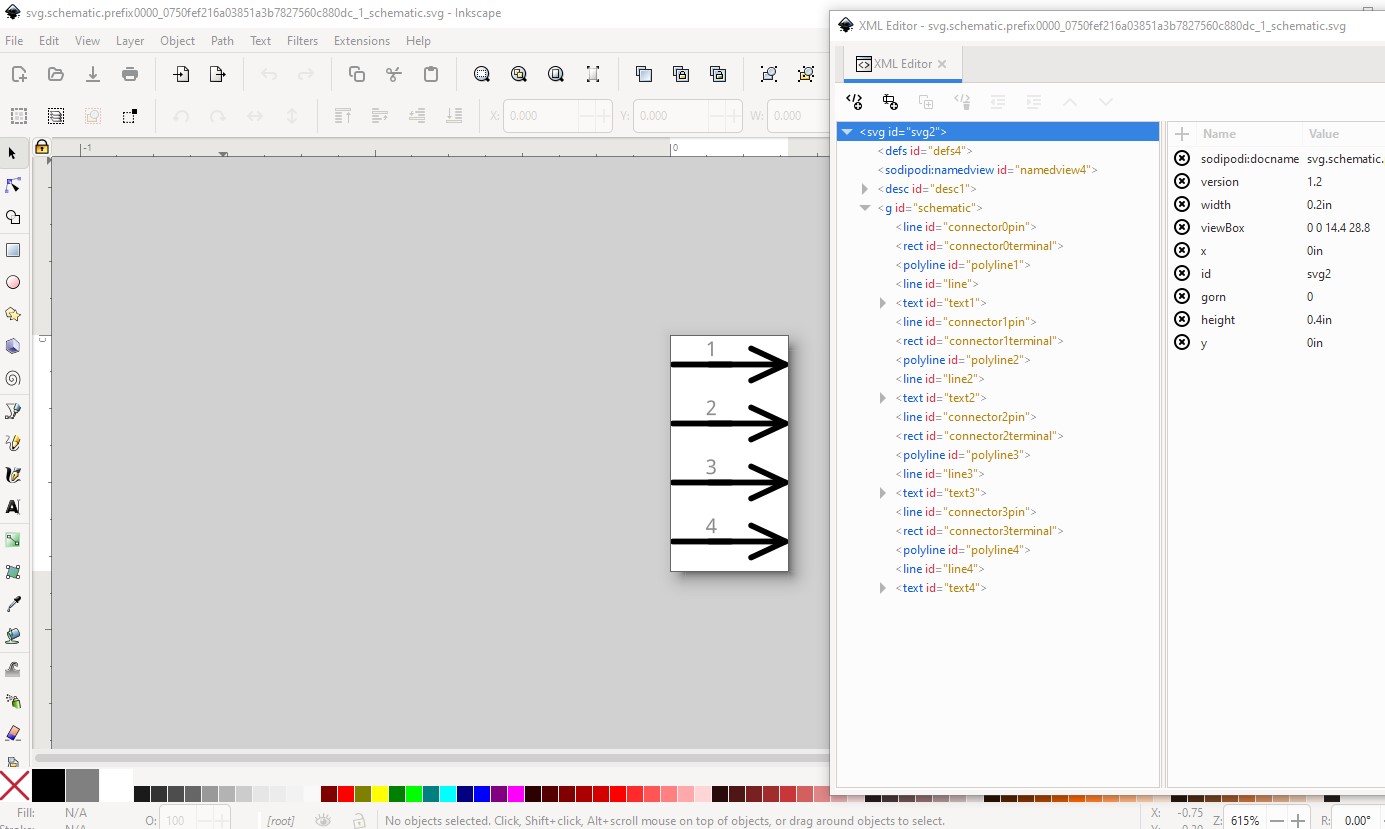
Thanks for the feedback… I’m pretty sure there are 4 connectors there in the .fzp connectors section that I posted. They are named ‘connector0’, ‘connector1’, ‘connector2’ and ‘connector3’. Or am I missing something here?

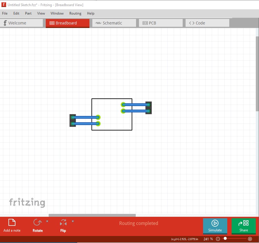
In the breadboard view only the top ones are shown, because I think you can not actually ‘flip’ a board in the breadboard view right? Or does a ‘breadboard0’ and ‘breadboard1’ layer work?

As for the shape, I have changed the shape to just a filled copper circle (instead of fill=“none” and with a copper stroke). The outcome was the same.

(I will post the .fzz file later :wink:)

Thanks for your feedback so far!

So without a .fzz, I made a part that does what you describe (which may or may not be what you wanted) and it appears to work as expected.

pcb svg in Inkscape

breadboard in Inkscape (note the pads are moved to not overlap as they may not overlap in breadboard to work!)

schematic

complete fzp file.

<?xml version='1.0' encoding='UTF-8' standalone='no'?>
<module moduleId="prefix0000_0750fef216a03851a3b7827560c880dc_1" fritzingVersion="0.2.2.b.03.04.2550" referenceFile="generic_male_pin_header_4_100mil.fzp">
  <version>4</version>
  <author>Fritzing Part-o-matic</author>
  <title>Generic male header - 4 pins</title>
  <label>J</label>
  <date>Fri Aug 23 2019</date>
  <tags/>
  <properties>
    <property name="family">test</property>
    <property name="hole size"/>
    <property name="Pins">4</property>
    <property name="Form">♂ (male)</property>
    <property name="Pin Spacing">0.1in (2.54mm)</property>
    <property name="Row">single</property>
    <property name="package">THT</property>
    <property name="Position"/>
    <property name="package">THT</property>
    <property name="layer"/>
    <property name="part number"/>
    <property name="variant">variant 1</property>
  </properties>
  <description>Generic male header</description>
  <views>
    <iconView>
      <layers image="breadboard/prefix0000_0750fef216a03851a3b7827560c880dc_1_breadboard.svg">
        <layer layerId="icon"/>
      </layers>
    </iconView>
    <breadboardView>
      <layers image="breadboard/prefix0000_0750fef216a03851a3b7827560c880dc_1_breadboard.svg">
        <layer layerId="breadboard"/>
      </layers>
    </breadboardView>
    <schematicView fliphorizontal="true">
      <layers image="schematic/prefix0000_0750fef216a03851a3b7827560c880dc_1_schematic.svg">
        <layer layerId="schematic"/>
      </layers>
    </schematicView>
    <pcbView>
      <layers image="pcb/prefix0000_0750fef216a03851a3b7827560c880dc_1_pcb.svg">
        <layer layerId="copper0"/>
        <layer layerId="silkscreen"/>
        <layer layerId="copper1"/>
      </layers>
    </pcbView>
  </views>
  <connectors>
    <connector type="male" id="connector0" name="pin1">
      <description>pin 1</description>
      <views>
        <breadboardView>
          <p svgId="connector0pin" layer="breadboard"/>
        </breadboardView>
        <schematicView>
          <p terminalId="connector0terminal" svgId="connector0pin" layer="schematic"/>
        </schematicView>
        <pcbView>
          <p svgId="connector0pin" layer="copper1"/>
        </pcbView>
      </views>
    </connector>
    <connector type="male" id="connector1" name="pin2">
      <description>pin 2</description>
      <views>
        <breadboardView>
          <p svgId="connector1pin" layer="breadboard"/>
        </breadboardView>
        <schematicView>
          <p terminalId="connector1terminal" svgId="connector1pin" layer="schematic"/>
        </schematicView>
        <pcbView>
          <p svgId="connector1pin" layer="copper0"/>
        </pcbView>
      </views>
    </connector>
    <connector type="male" id="connector2" name="pin3">
      <description>pin 3</description>
      <views>
        <breadboardView>
          <p svgId="connector2pin" layer="breadboard"/>
        </breadboardView>
        <schematicView>
          <p terminalId="connector2terminal" svgId="connector2pin" layer="schematic"/>
        </schematicView>
        <pcbView>
          <p svgId="connector2pin" layer="copper0"/>
        </pcbView>
      </views>
    </connector>
    <connector type="male" id="connector3" name="pin4">
      <description>pin 4</description>
      <views>
        <breadboardView>
          <p svgId="connector3pin" layer="breadboard"/>
        </breadboardView>
        <schematicView>
          <p terminalId="connector3terminal" svgId="connector3pin" layer="schematic"/>
        </schematicView>
        <pcbView>
          <p svgId="connector3pin" layer="copper1"/>
        </pcbView>
      </views>
    </connector>
  </connectors>
</module>

and the part file

test.fzpz (3.4 KB)

which produces this output in Fritzing

which appears to do what you want (in a way Fritzing will accept.) If you upload the .fzz file I can probably tell you what is wrong with your part or you can look over this one to see what I did.

Now the associated gerber output

all layers

bottom layer

top layer

which indicates the part works correctly.

Peter

Wow thanks for the effort you put into this Peter!
Here is my fzz file:

opposite pads issue.fzz (4.1 KB)

I really hope you can get this working!
Thanks in advance!

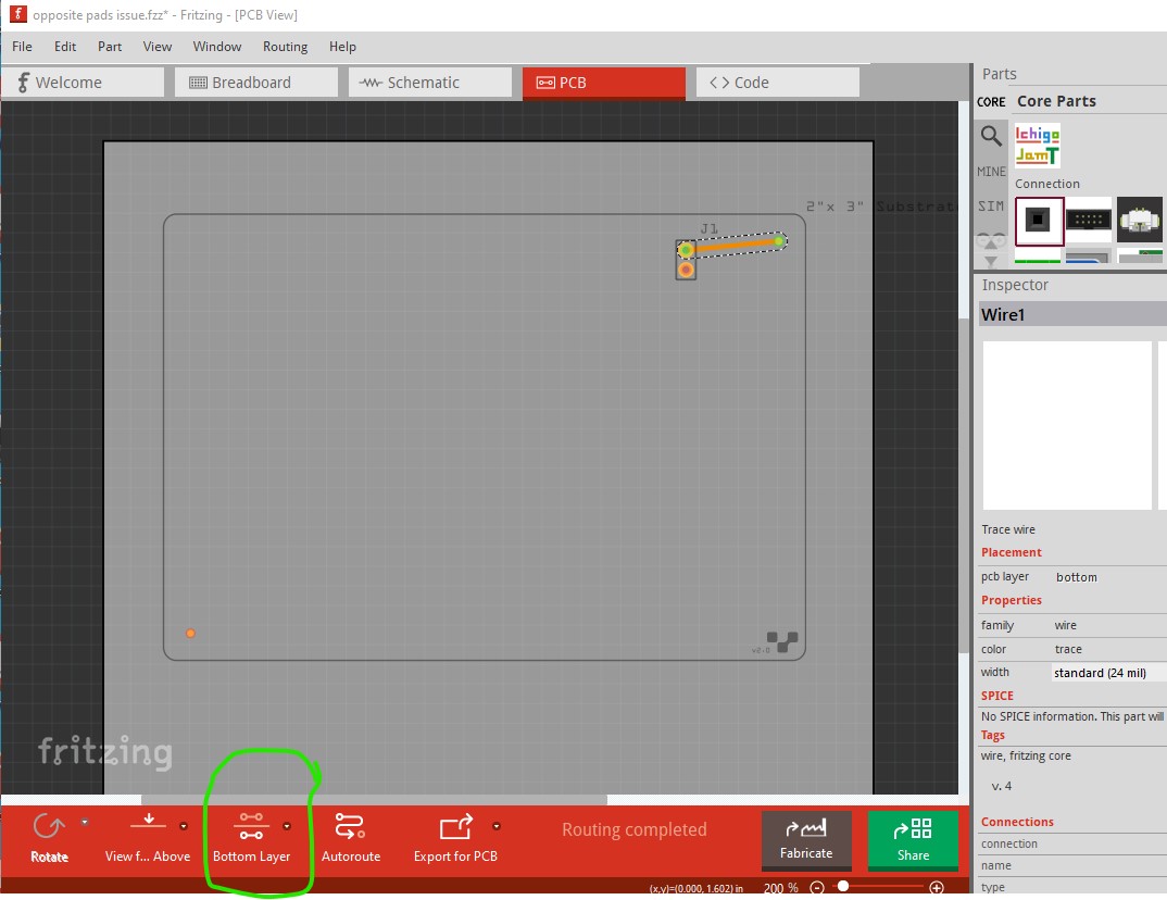
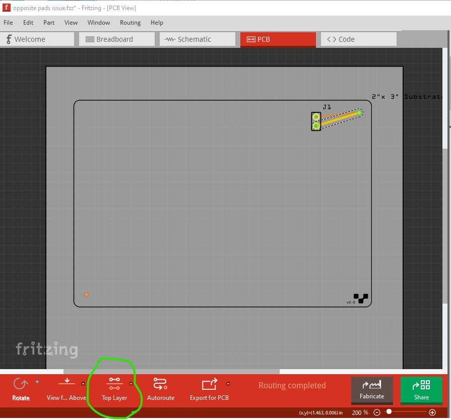
Your part is in fact working but with some limitations. Because this is in effect a SMD part you can’t select between the layers. Because both pads are not defined in breadboard you can’ t (as I did in my sketch) make a connection in breadboard which will reflect in to pcb on the correct layer, so you need to select which layer you want to connect manually. Normally this field would change between top and bottom layer. Here it is disabled (as it is in my part) because the part is SMD and only exists on one layer.

To make the correct connections in pcb you need to change the layer setting from both to bottom to route the bottom layer on the bottom layer to the bottom pad.

then change the layer to top to route the top layer pad on the top layer to the top pad.

then your part works as intended (although only one connection will show in breadboard unless you define both pads as I did.) This is a limitation in how Fritzing operates.

Peter

Hi Peter,

Thanks for figuring it out! I’m glad to hear my part was working, I was able to reproduce your results but must say that the pop-up is not consistent and turned out to be what was confusing me in the first place.

You see, connector 0 and 1 are on the top layer and 2 and 3 are on the bottom.
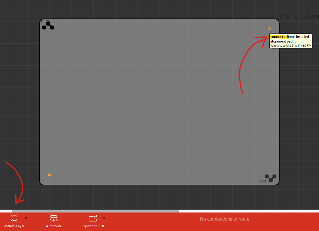
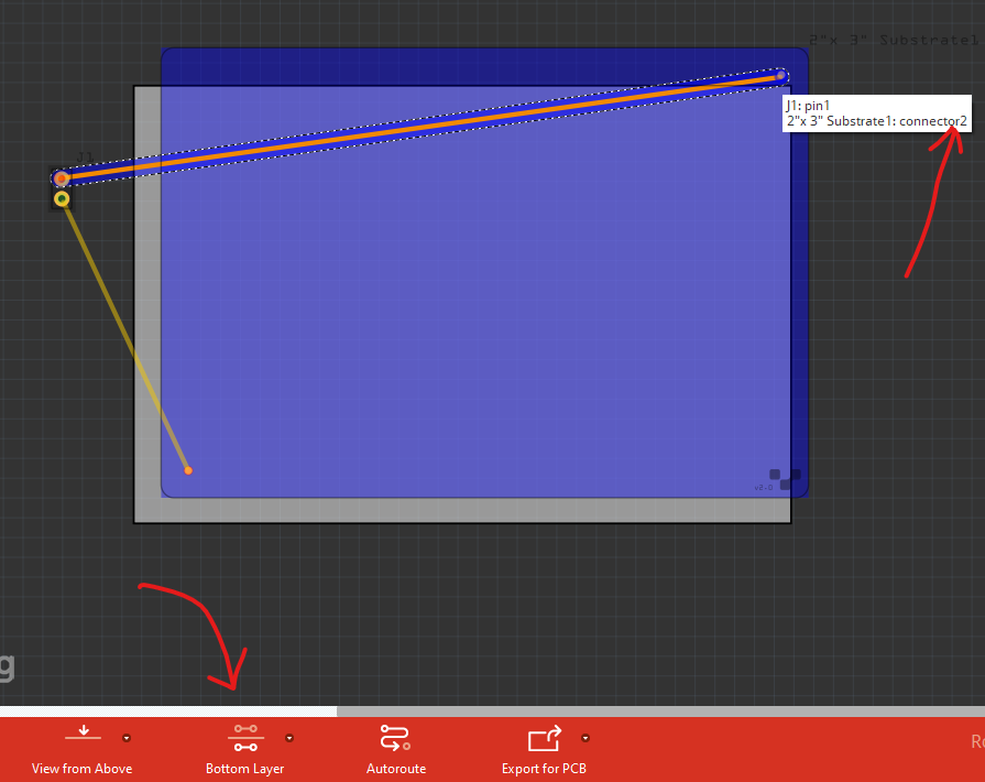
But with bottom layer selected, if I hover the cursor over the connector it shows this (as in my original post):

But, when dragging a wire to the connection it shows this:

Anyway, thanks for putting so much effort in figuring this out!
I’ll manage with this info and will ignore the confusing pop-ups​:stuck_out_tongue_winking_eye::+1:t2:

Thansk!

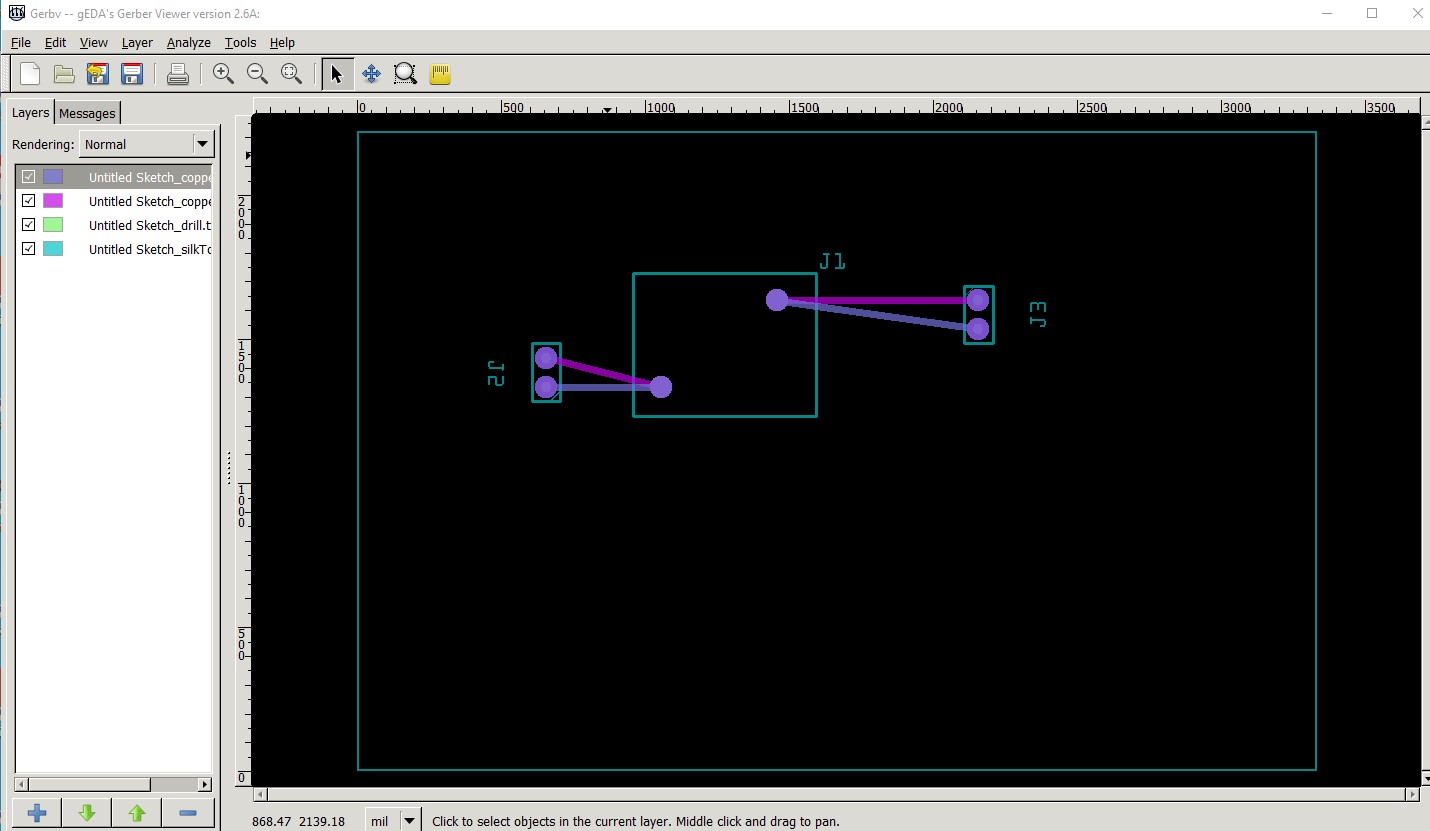
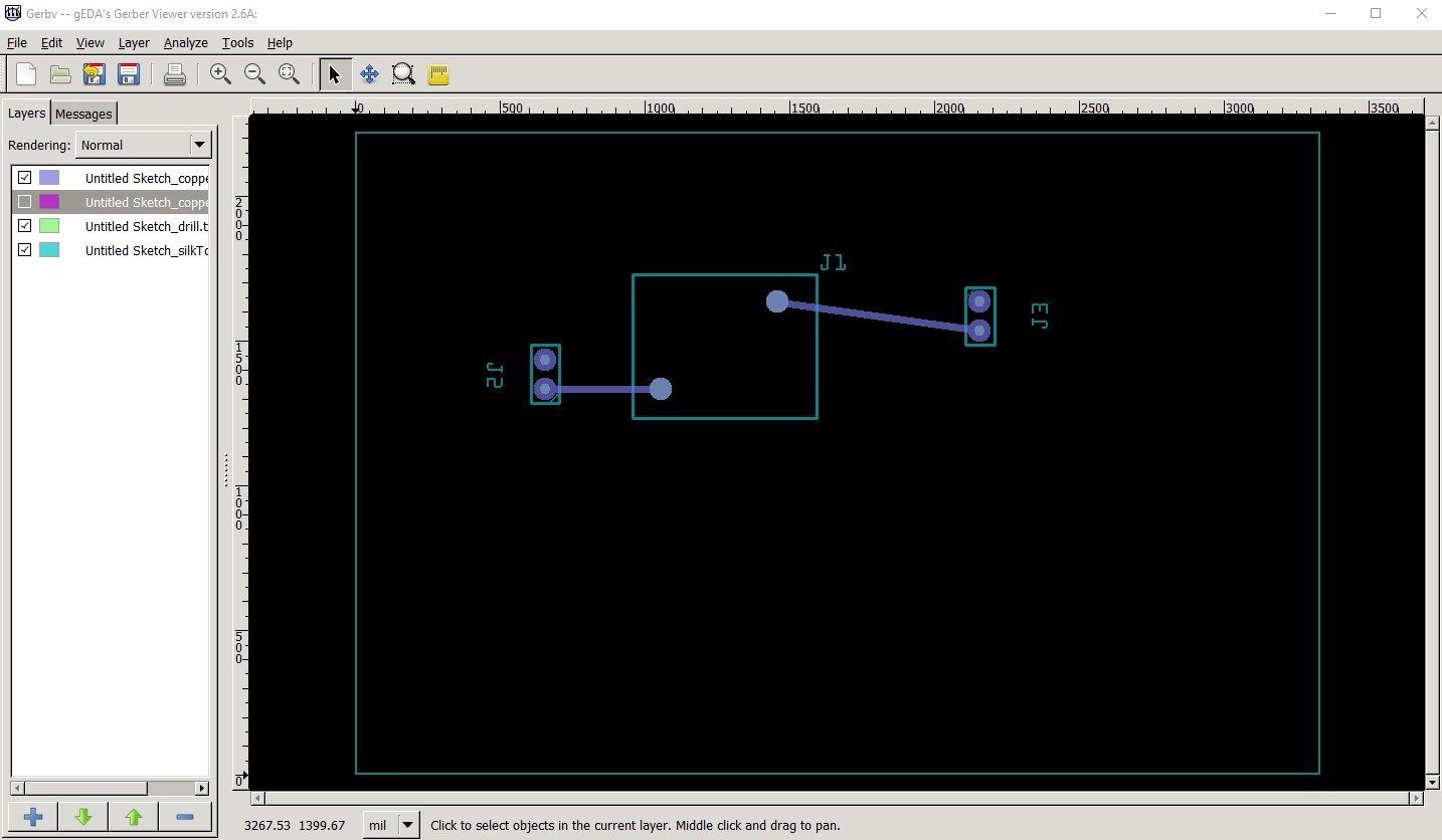
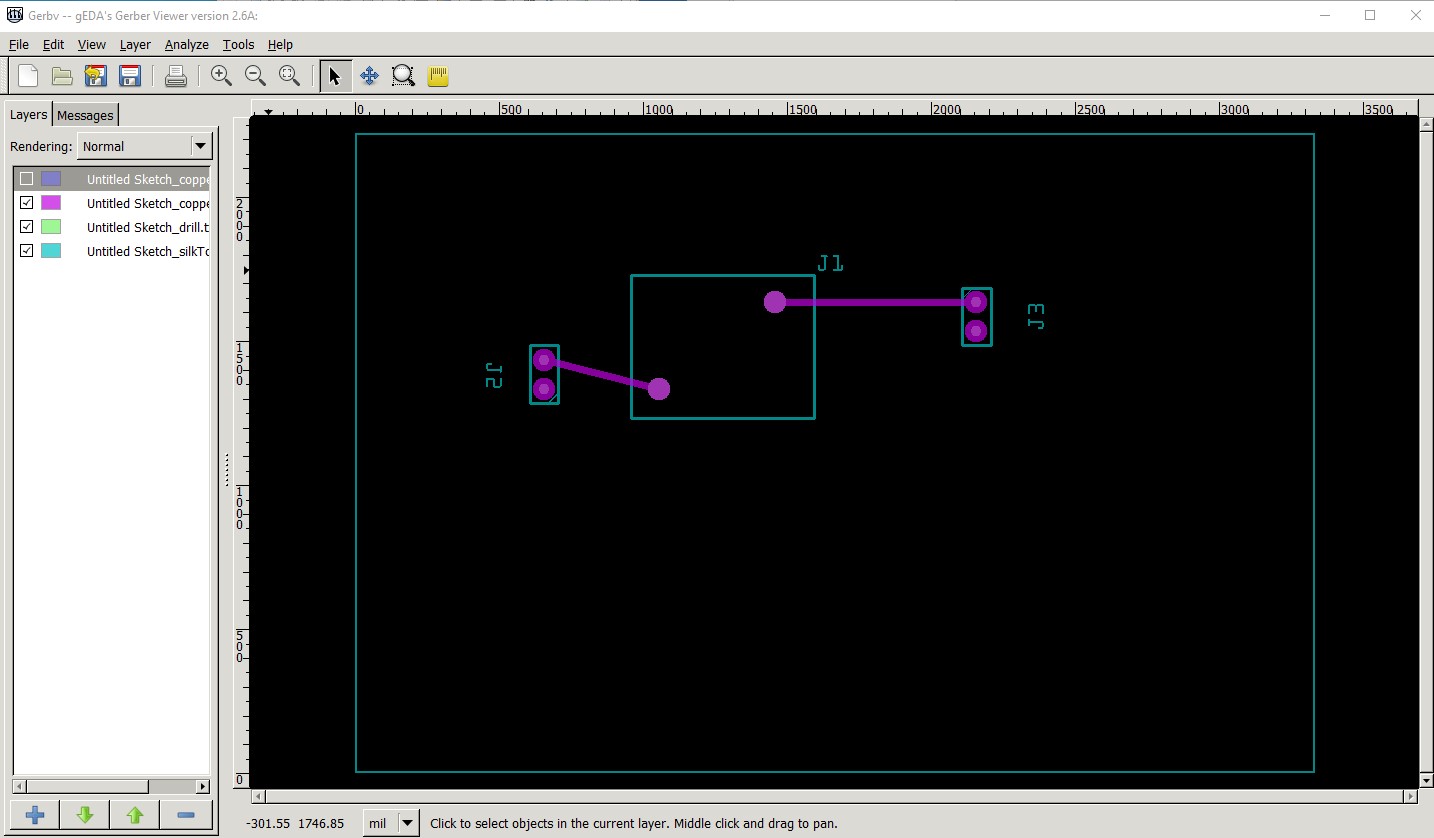
The first image has two pads to choose from and will (perhaps randomly, perhaps some criteria I don’t know) choose one to display the data for. The second image has a trace on bottom layer and will thus select the bottom layer pad that it connects to to display. The bottom trace is top layer and will display the top layer pad it connects to.

Peter