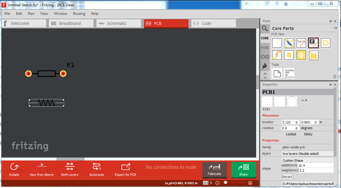
Sometimes I want to create a resistor symbol on the PCB which is larger than the maximum
available pin spacing which is 800mil.
Up to now I solve this by just creating two vias which have their distance matching that larger resistor size. But then there is no resistor symbol drawing in the silk screen possible on that place so I create a PCB text with just the resistor number between those two vias.
Is there a possibility to create a resistor drawing symbol (or simply a rectangle) in the silk screen?
Hope I made myself clear enough.
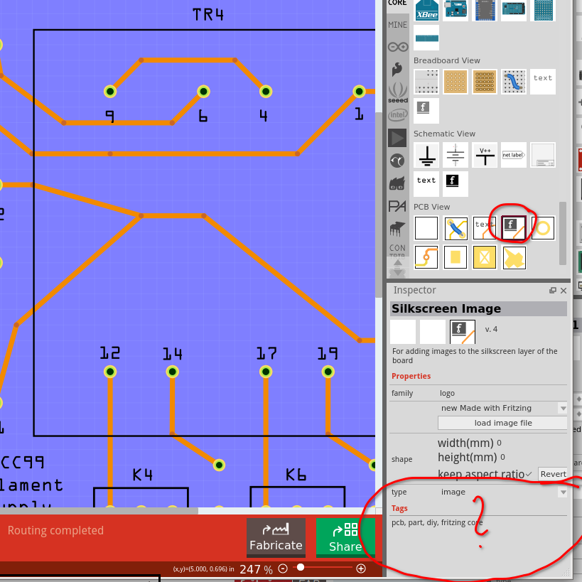
Hello, Custom silkscreen is very simple to make…
First, create the desired image in simple Black & white color…
Best to make in “svg” or “png” format…
SVG: just create the image image in any color…
PNG: without transparency, background in black, image in white (simply in MS-paint)
Then, select the silkscreen option in fritzing, and upload your “svg” or “png”…
resize it …
PNG:

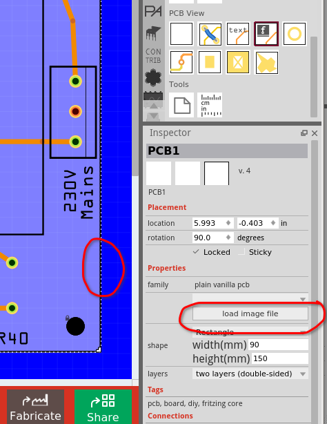
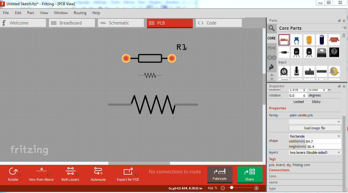
Thanks Blue for trying to help me but it leaves me still puzzled how to import an .svg image into that silkscreen option in my PCB.
- I made with Inkscape a simple square as a test image.
- selected the silkscreen image logo in fritzing and dragged it into my PCB drawing.
But then? tried several things to get the .svg image into that logo but I failed.
What am I doin wrong?
Here is how I did this using Inkscape. For maximum laziness start with the schematic of a resistor, as the base:
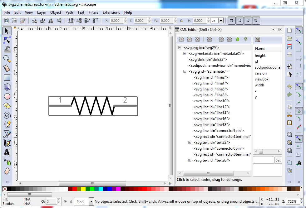
to get the shape you want. Now in Inkscape (or one of the other svg editors)
ungroup
delete the text for 1 and 2
delete connector0terminal and connector1terminal
change the id field of connector0pin and connector1pin to line
edit select all resize drawing to page.
group
set the group id to silkscreen
create an invisible rectangle slightly larger than the resistor image for the board outline to leave this as the svg:

and the actual svg (the forum won’t load it so you need to unzip silkscreen-svg.fzpz to get the svg)
silkscreen-svg.fzpz (931 Bytes)
However that appears to use the board outline of the custom shape for the entire board and won’t change it. So I don’t think this will do what you want (I haven’t played with silkscreen icons much though)
Peter
After Dragging fz logo, you have to upload your image…
Also, you can make silkscreen part as peter said…
Anyway, you want larger than 800mil resister…
I posted a 1200mil ceramic 5w resistor before…
Is this helps: 81. Resistor 5W (ceramic).fzpz (4.6 KB)
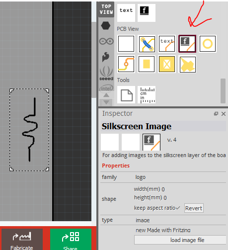
Ah that is what I missed! As @blue said, just import my silkscreen.svg file as an icon and that will work. It no longer sets the board outline and you can resize the resistor image by changing the shape parameter in Inspector. The svg likely doesn’t need the board outline group, but it doesn’t seem to care either.
!
The bottom two images are my svg, duplicated then with the bottom one resized in Inspector. This is what I was expecting to happen, but I selected silkscreen image in stead of logo and silkscreen image wants a board outline. Note the grey on the resistor will come out the same color as the black on the silkscreen (I or you should change that in the svg …)
Peter
@Blue and Peter:
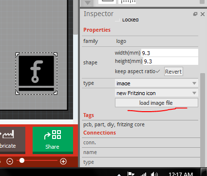
I simply overlooked “load image file” at the bottom of my screen! Do not know why but after Blue showed it, I immediately noticed it. Must be my age… 
Now I can try to find my way and experiment further. Will let you know the results.
Joe.
Update : Sometimes that “load image file” does not show up ! That is perhaps why I missed it.
I believe you have to have something in the sketch selected for it to show up. It can’t change things in Inspector (actually in the parts bins) but only in a sketch.
Peter
Peter, I mean it does not show up in the Inspector, so I cannot select it to import the sketch.
When I close Fritzing and start it up again then, after selecting that “f” icon and drag it into the PCB drawing, it does show up, then I can import the sketch.
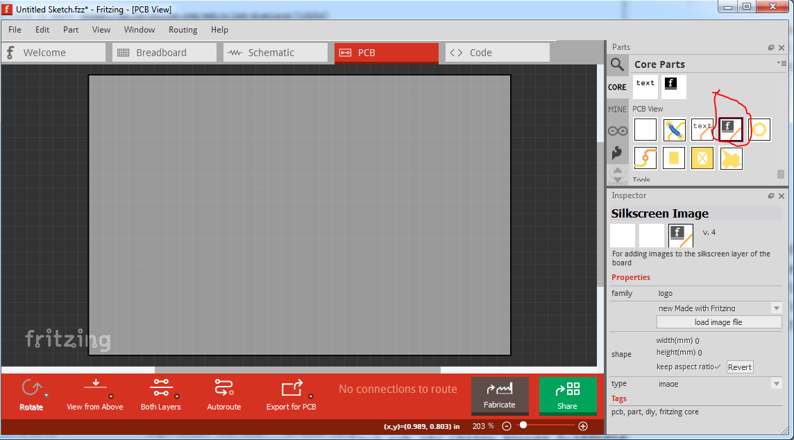
Do you mean that this icon isn’t showing up?
If so it sounds like you have corruption in the user directories and a clear will probably help (although you will need to backup and restore your mine parts bin)
There are two user directories (with your parts and the parts database) which don’t get touched during an install (to not affect your sketches during upgrades). On Windows they are in
c:\users\username\AppData\Fritzing\roaming\Fritzing (which is a hidden directory so you need to enable hidden directories in explorer) and
c:\Users\username\My Documents\Fritzing (where username is your windows id)
If you don’t have any parts or sketches you want to keep you can just delete those two directories and Fritzing will recreate them, or you can move them aside by renaming them if you wan to keep something in them.
linux
~/Documents/Fritzing/parts
~/.config/Fritzing
Mac
/Users/username/Documents/Fritzing/parts
~/.config/Fritzing
Peter
No I mean THIS is sometimes not showing up:
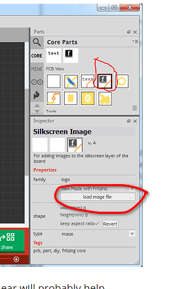
I am using Linux KDE5.
Perhaps it’s a simple oversight…
You need to click on the PCB to activate the PCB’s Inspector. If PCB is not selected, the Inspector won’t show.
Do not (yet) know why but now, whatever I do, that “load image file” is always showing up when I click or even hoover over that “f” symbol in the PCB View part…
But if the problem appears again I will try your idea. Thanks anyway.
Joe.
I haven’t been able to reproduce this either on Windows or Linux (my Ubuntu 18.04 development system.) Is it possible the box is there but just white? There is a bug report open that Linux changes some of the Inspector (I think!) text to white an a white background (which I have seen Windows do on occasion too) and the text becomes basically unreadable.
Peter
Thanks Peter, I will consider that (white text) as a possibility and the moment it happens again I will look into it.
By the way my linux distro is PCLinuxOS KDE5 and PCLinuxOS MATE, I have fritzing running on both desktops.