Creating a new breadboard

Dear all,

I’ve just started to learn fritzing and electronics in general. For my first builds, I’ve created a few simple guitar amplifiers using ‘Electrocookie’ breadboards. These are not available in fritzing, and I’d like to make my own.

I’ve looked if they are available somewhere, and although there is a project which supposedly has these boards, these do not actually have the boards’ graphics and the holes are not in the proper positions.

Similar questions have been asked by other users, but the general response is that building breadboards is tricky. The linked tutorials have not been very helpful. I am good at working with inkscape, and I don’t mind putting in work to build the boards myself.

Can anyone tell me how to do it?

Thanks!

1 Like

Electrocookies appear to be a variety of perf board not a breadboard. Creating one is even more difficult than a breadboard as it requires a code change in Fritzing (new breadboards can be created, if you know enough, without code changes!) It should be possible (but not particularly easy) to modify a breadboard to look like a Electrocookie, but you would need a different part for each size you want if you don’t want to make a code change. Making breadboards has not been documented because there isn’t a lot of demand to do it (and when someone wants one I usually do it, as that is easiest!) I’ve needed to do it several times and therefore learned how to do it. To be successful you need to be familiar with the xml that creates parts and know the various special settings (which are undocumented so far) that are required to create breadboards. If you have one of the Electrocookies (there appear to be various sizes) that you want I’ll have a look at what it would take.

Peter

I don’t want to Dissuade users from using Fritzing - it’s good for learning, single and two layer PCB’s and BreadBoard graphic representation. But, it’s PCB and Part making lack user-friendliness and quickness.

I used Fritzing for a few years and built many PCBs with it. However, too often I needed to spend more time than I wanted in making parts and going back and forth between Inkscape and Fritzing.

Finally, I realized it was time to upgrade to another program. I chose Kicad. It too, has some user-unfriendliness. However, its full power in making PCB and schematic is not to be overlooked.

99.9% if Kicad users aren’t interested in BreadBoards but, being a Geek, I jimmied-up BreadBoards in Kicad. No need for other programs (Inkscape, etc. But, can use them in combination, if desired. I used FreeCAD for the 3D-Modeling (just for 3D Graphic).

Generally speaking, there are two types of BreadBoard -actually, only One, type, the other is called PerfBoard. BreadBoards have fully-connected strips of Pads and PerfBoards have individual Pads.

Examples of some…

Dear Peter, opera_night

Thank you for your replies. I guess that technically, the Electrocookie boards I use are stripboards. I use them to transform breadboard projects into portable devices (guitar effects pedals). For use in fritzing, it would be sufficient for my uses if they function as breadboards.

I use the mini (5+5)*17 version and the larger (5+5)*30 version. They come in six colors, and I’d like to have each color for both sizes to be able to document the things I’ve built. If you’d be willing to make these that would be great.

In the attachment is an SVG that has the proper sizes for the mini boards. The larger ones I still have to make. Please let me know if these are suitable for an implementation.

Aside, thanks for the Kicad suggestion, but first I’ll learn fritzing :slight_smile:

ElectroCookie_Mini

This should do to make a part. Are the pads connected together (i.e. A-E connect to each other like a breadboard) or are they like perf board each an individual pad with no other connections? The various colors aren’t a problem, that is a change of a single background color to make a new part with a different color once the first is done.

Peter

Great - there are connections: with the board in landscape orientation, each column is separate. Within the columns, holes a-e are connected, and so are f-j. Just like a breadboard.

OK, I’m working on your svg and will document as I go as an example of how to make a breadboard (or breadboard like part.)

Peter

OK here is a part and how I made it.

ElectroCookie-red-17.fzpz (6.8 KB)

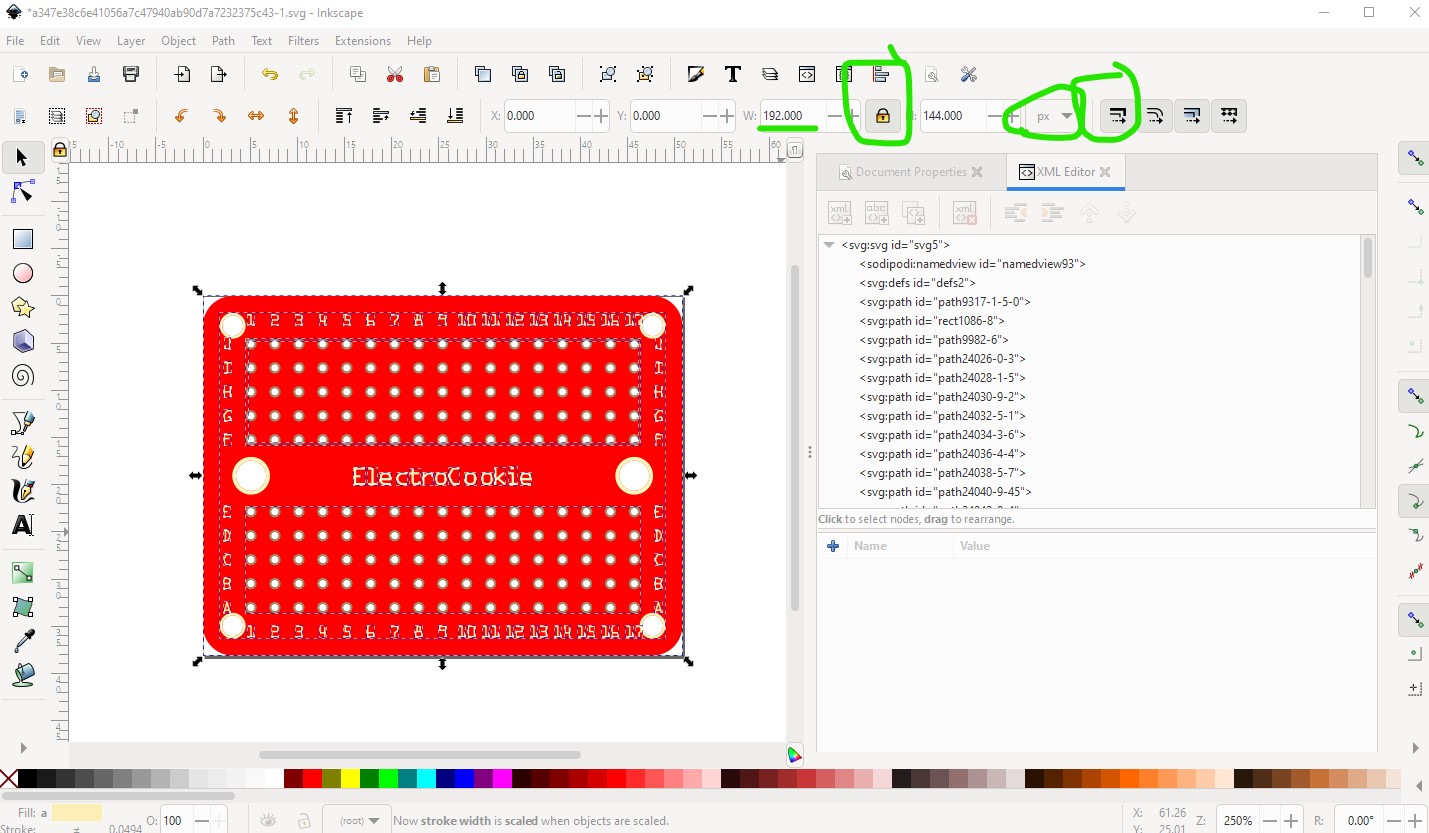
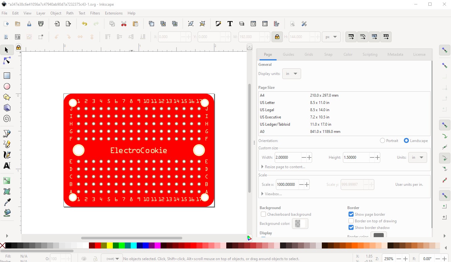
Start from a347e38c6e41056a7c47940ab90d7a7232375c43.svg above, and cut it down to a single instance of the board from several.

a347e38c6e41056a7c47940ab90d7a7232375c43-1

then ungroup the svg and change it to the desired scale (where 1 drawing unit = 1/1000 in.) To do that set dimensions to px and copy the width and save it. Lock width to height and enable scale stroke width when scaling.

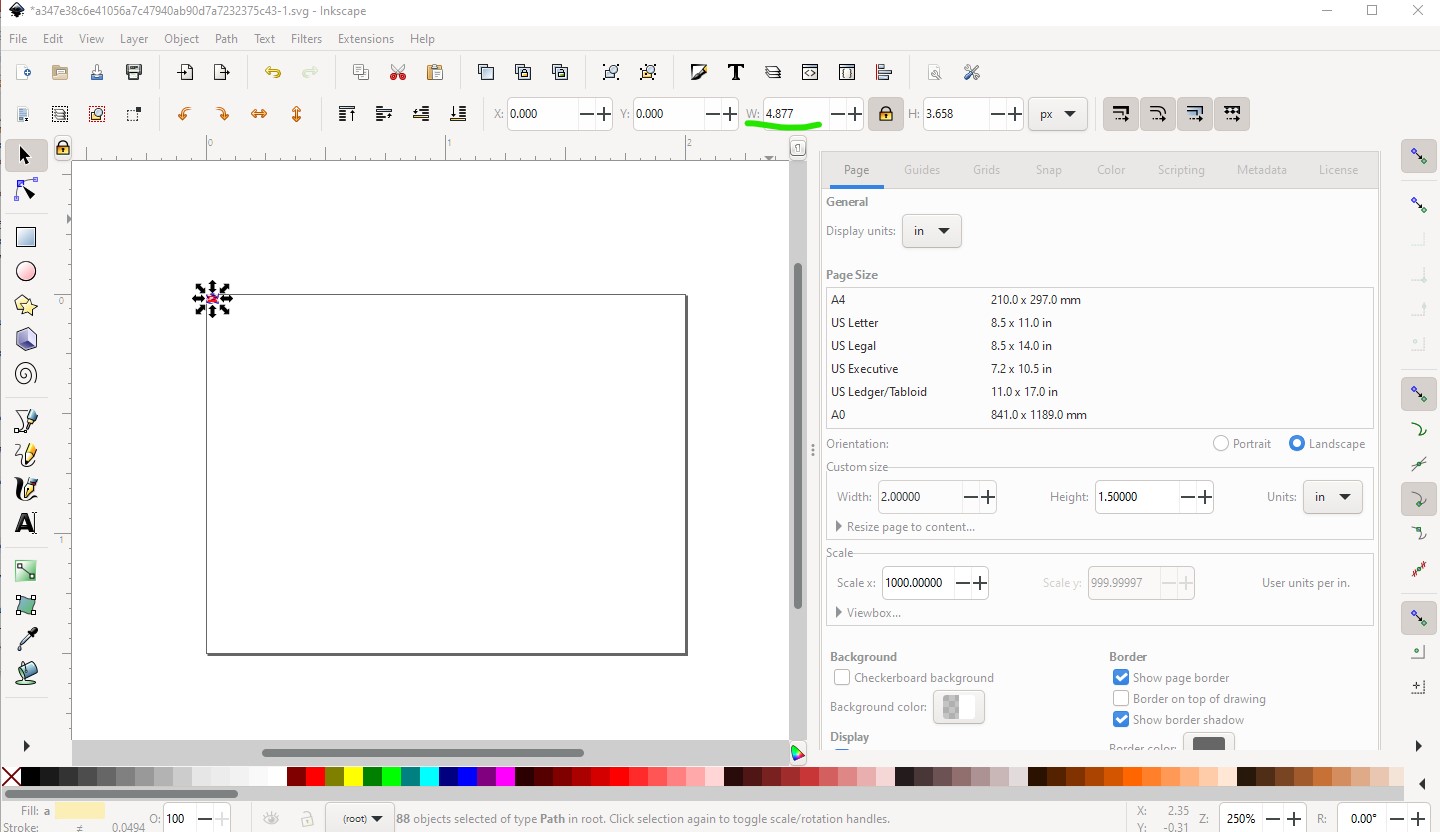
Then do Edit->select all to do the entire svg and in document properties change the dimensions both to inches

then change the scale to 1000 (note this is Inkscape 1.1.2, earlier versions use a different scale value!)

then set the width back to 192px to complete the scale.

here is a copy of the rescaled svg for reference

a347e38c6e41056a7c47940ab90d7a7232375c43-2

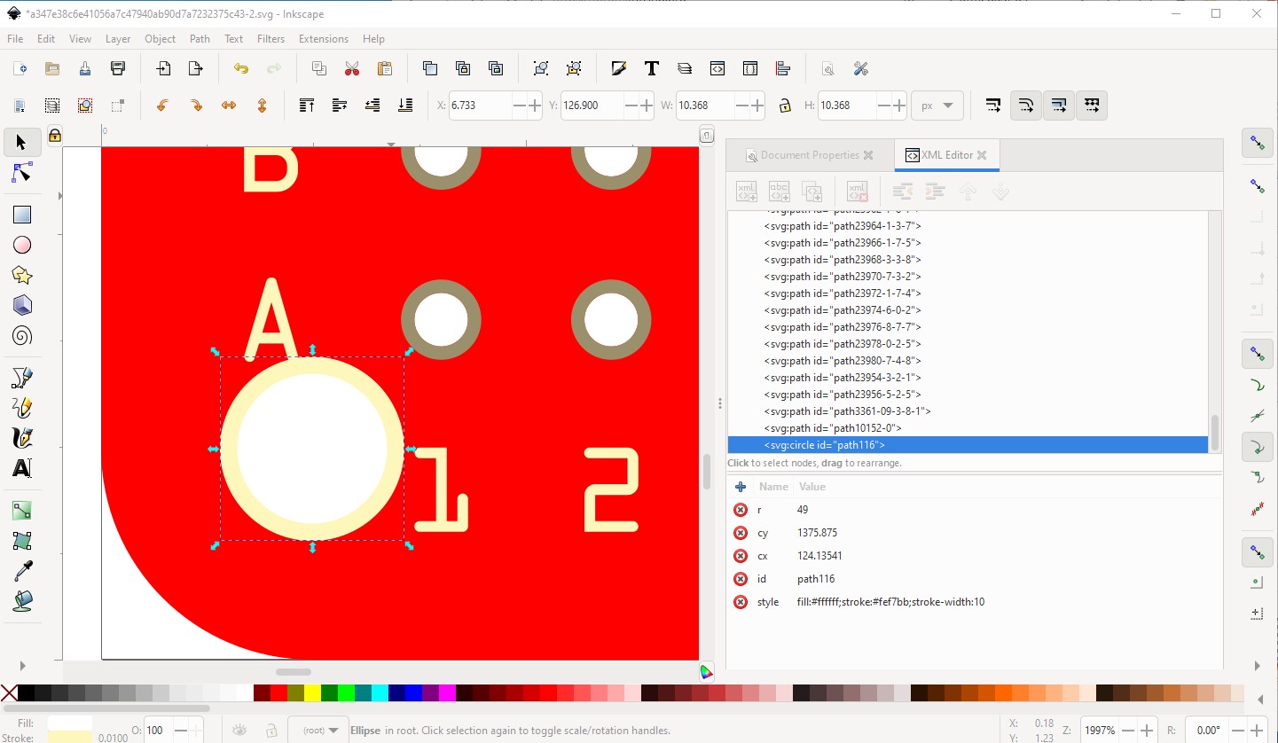
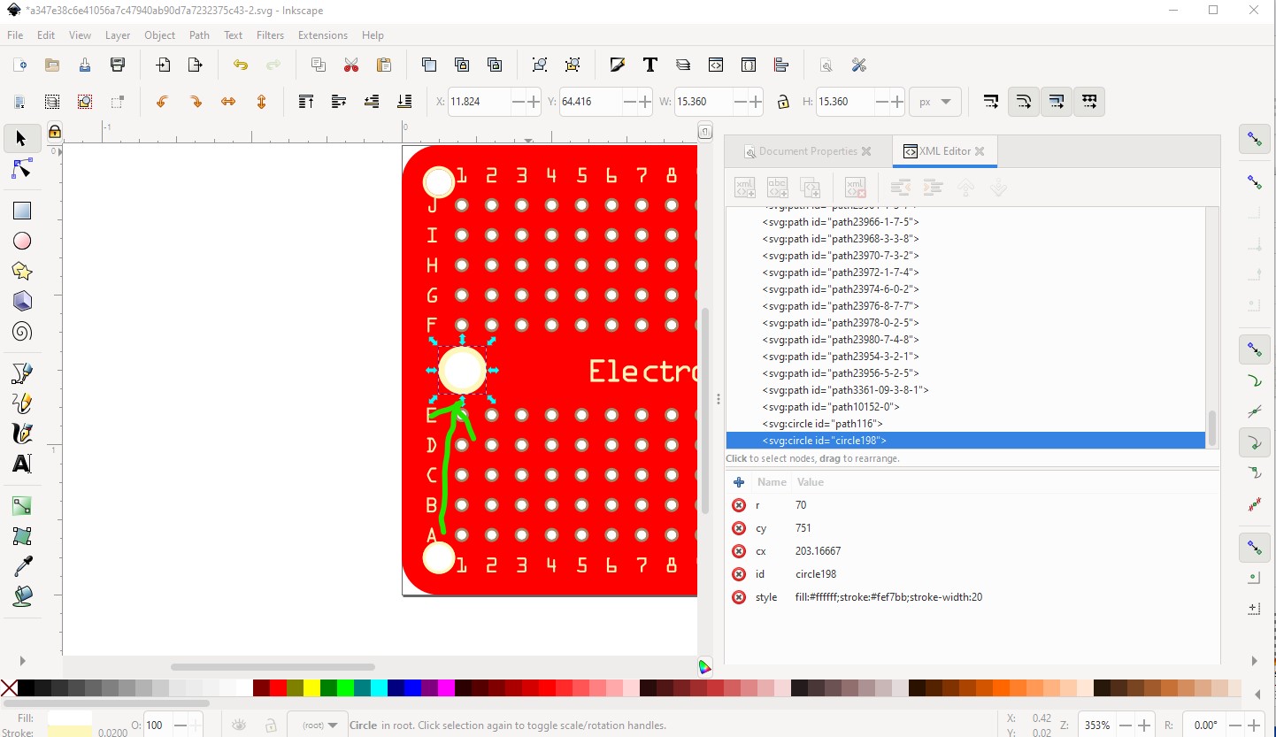
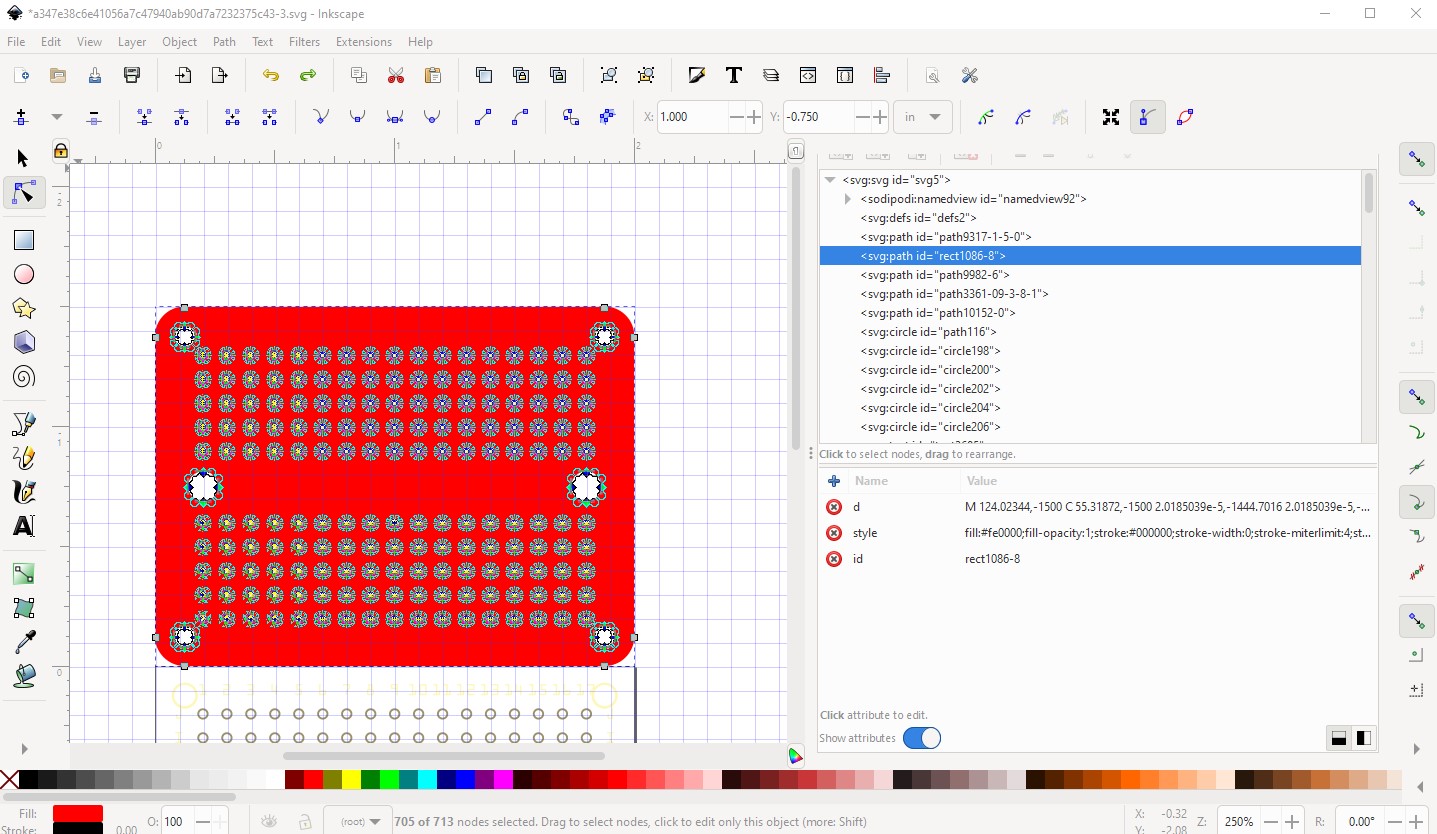
Now before moving on to connectors (which for placement reasons want to be the last thing done so they end up at the bottom of the svg), replace the mounting circles with equivalent circles (this isn’t really necessary, but I find it easier to change a circle if I need to later than edit a path!)

here I overlaid a circle on the bottom circle then duplicated it and moved it to the next circle up. It needs a larger stroke width and an increase in radius like this:

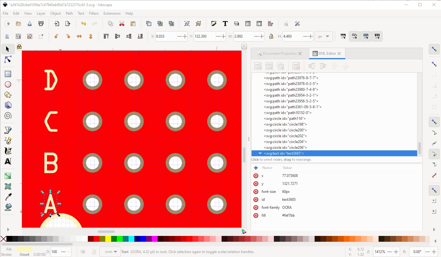
do the same for all the other circles that are not connectors. Then replace the text as paths with OCRA text like this

and repeat for the rest (deleting the current paths as I go.) Duplicate and move the left text to replace the right and the top to replace the bottom. Then delete all the holes from the path by moving the path up then deleting all the holes.

to leave only the path, then move it back in to position.

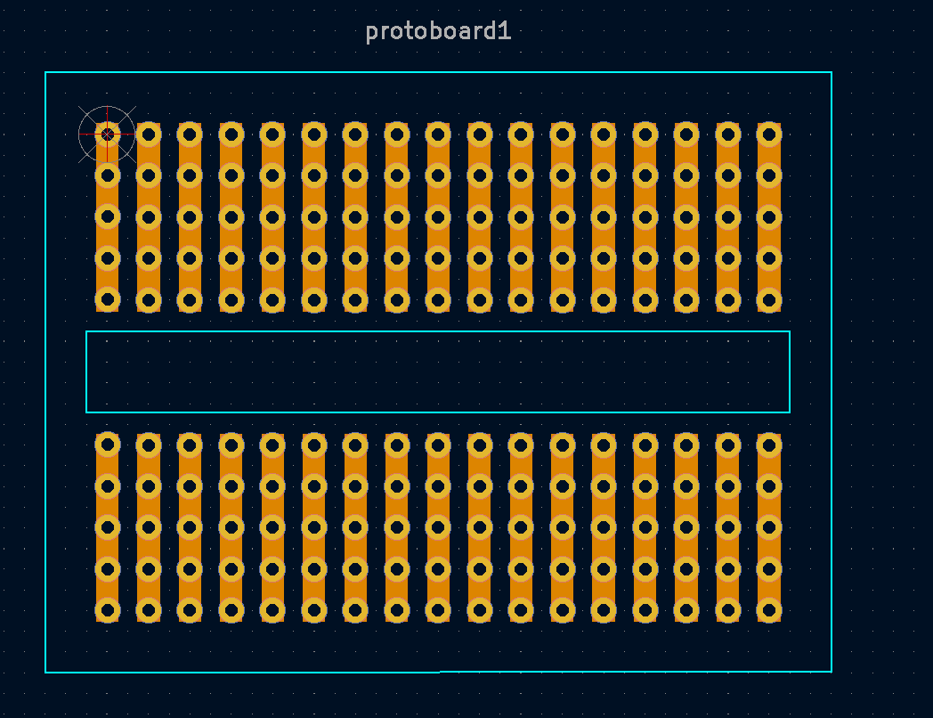
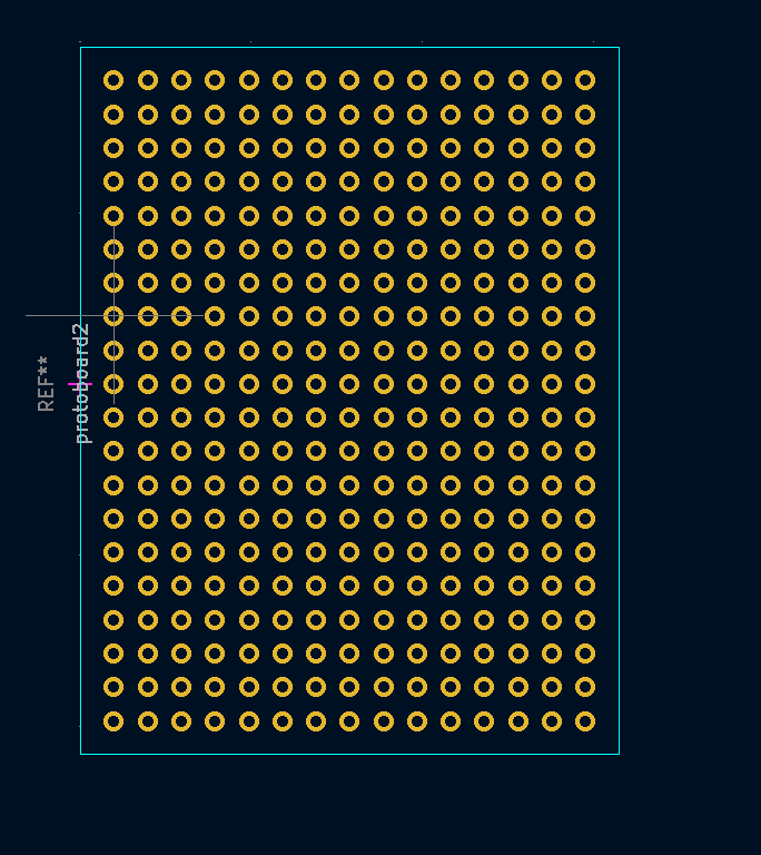
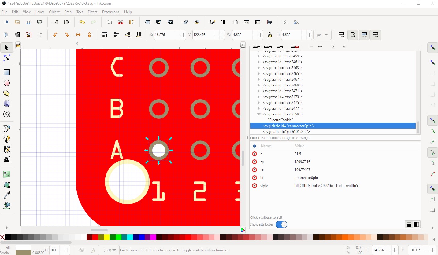
Now convert the paths to individual pads as needed by Fritzing by creating a pad that has a 0.038in (suitable for 0.1in headers) pad and align it on the first pad. Fritzing needs each pad to be an individual circle (or other shape) to define the connections.

Now move the path containing the other pads up one level in xml editor and set the id of the new pad to connector0pin (Fritzing convention) to indicate the first pin. I have scripts which will renumber the pads automatically to make less typing. Although it doesn’t matter here (because breadboards don’t have a pcb view) I set the pad to have a stroke width of 5thou in (the normal is 20thou in) and the radius to 21.5 to produce a 0.038in hole suitable for a 0.1 header if we were making pcb. The hole size calculation in Inkscape is hole-size = pad-diameter - (2 * stroke-width) so in this case 0.048in pad diameter and 5thou stroke width create a 0.038in hole. Now duplicate the pad and move it up in Y by .1 in by clicking on the - on the y coord in the tool bar to set the next pin (I didn’t bother to set the id as a script will do that later.) Repeat for all the other pads. Then save the svg and run it through

$ SvgSetConnectorsbb.py a347e38c6e41056a7c47940ab90d7a7232375c43-3.svg

*** Process a347e38c6e41056a7c47940ab90d7a7232375c43-3.svg ***

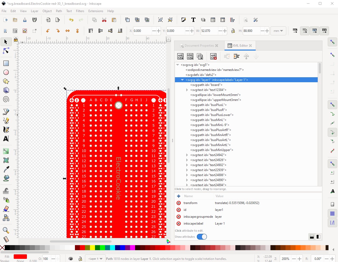
to renumber the pins. Then group the entire svg and set the layerId to breadboardbreadboard and rename the svg to

svg.breadboard.ElectroCookie-red-17_1.breadboard.svg

to be in the correct Fritzing naming format for a .fzpz file. That results in this

which is the breadboard svg ready for use. Now we need to create a .fzp file for the part. This is where the undocumented parts of making a breadboard occur (although the breadboardbreadboard layerId in the svg is also part of this!) Here I started with the breadboard2 fzp file and will modify it to suit the current task. First rename it from

part.breadboard2.fzp

to

part.ElectroCookie-red-17_1.fzp

Then change the moduleId (which must be unique in Fritzing and in this case end in “ModuleID” to alert Fritzing this is a breadboard. So change

	<module moduleId="Breadboard-RSR03MB102R-P-ModuleID">

to

	<module moduleId="ElectorCookie-red-17_1-ModuleID">

Set the version from 4 to 1 (as this is the first version of this part.)

<version>4</version>

to

<version>1</version>

change the tirle to match this part giving the color and the size to differentiate it.

<title>ElectorCookie red 17</title>

family name needs to remain Breadboard (it is one of the trigger values!)

<property name="family">Breadboard</property>

but the size needs to select this color and length in Inspector so change

<property name="size">full+ Rev Num</property>

to

<property name="size">ElectroCookie red 17</property>

change

<description>A breadboard for easily prototyping circuits. This version is modified to be a loadable part and was rescaled to be on a .1 grid in Inkscape 0.91.</description>

to

<description>ElectroCookie solderable perfboard, red 17 columns.</description>

change

<iconView>
  <layers image="icon/breadboardicon.svg">

to

<iconView>
  <layers image="breadboard/ElectroCookie-red-17_1_breadboard.svg">

change

<breadboardView>
  <layers image="breadboard/breadboard2.svg">

to

<breadboardView>
  <layers image="breadboard/ElectroCookie-red-17_1_breadboard.svg">

change

<schematicView>
  <layers image="breadboard/breadboard2.svg">

to

<schematicView>
  <layers image="breadboard/ElectroCookie-red-17_1_breadboard.svg">

change

<pcbView>
  <layers image="breadboard/breadboard2.svg">

to

<pcbView>
  <layers image="breadboard/ElectroCookie-red-17_1_breadboard.svg">

change

<connectors ignoreTerminalPoints="true">
<connector id="pin1A" name="pin1A" type="female">
  <description>breadboard socket</description>
  <views>
    <breadboardView>
      <p layer="breadboardbreadboard" svgId="pin1A"/>
    </breadboardView>
    <schematicView>
      <p layer="breadboardbreadboard" svgId="pin1A"/>
    </schematicView>
    <pcbView>
      <p layer="breadboardbreadboard" svgId="pin1A"/>
    </pcbView>
  </views>
</connector>
... (many more!)

to

<connectors ignoreTerminalPoints="true">
</connectors>

then load a script created connector file of 170 connectors like this:

<connectors ignoreTerminalPoints="true">
  <connector id="connector0" type="female" name="Pin 0">
    <description>breadboard socket</description>
    <views>
      <breadboardView>
        <p svgId="connector0pin" layer="breadboardbreadboard"/>
      </breadboardView>
      <schematicView>
        <p svgId="connector0pin" layer="breadboardbreadboard"/>
      </schematicView>
      <pcbView>
        <p svgId="connector0pin" layer="breadboardbreadboard"/>
      </pcbView>
    </views>
  </connector>
  ... (169 more)

then convert the buses from

<buses>
  <bus id="bus1A-E">
    <nodeMember connectorId="pin1A"/>
    <nodeMember connectorId="pin1B"/>
    <nodeMember connectorId="pin1C"/>
    <nodeMember connectorId="pin1D"/>
    <nodeMember connectorId="pin1E"/>
  </bus>
<bus id="bus1F-J">

to

<buses>
  <bus id="bus1A-E">
    <nodeMember connectorId="connector0"/>
    <nodeMember connectorId="connector1"/>
    <nodeMember connectorId="connector2"/>
    <nodeMember connectorId="connector3"/>
    <nodeMember connectorId="connector4"/>
  </bus>
<bus id="bus1F-J">

to create the necessary buses. Then save the fzp file and run it through FritzingCheckPart.py to make sure it is correct:

$ FritzingCheckPartw.py part.ElectroCookie-red-17_1.fzp

which produces a number of warnings (expected, it isn’t used to dealing with breadboards!) but no errors. So create the fzp file by zipping

part.ElectroCookie-red-17_1.fzp

and

svg.breadboard.ElectroCookie-red-17_1_breadboard.svg

into

ElectroCookie-red-17.fzpz

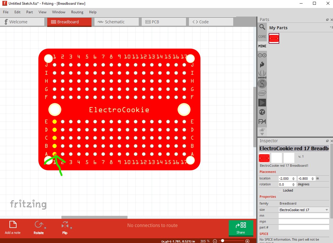
load that in to Fritzing and test it.

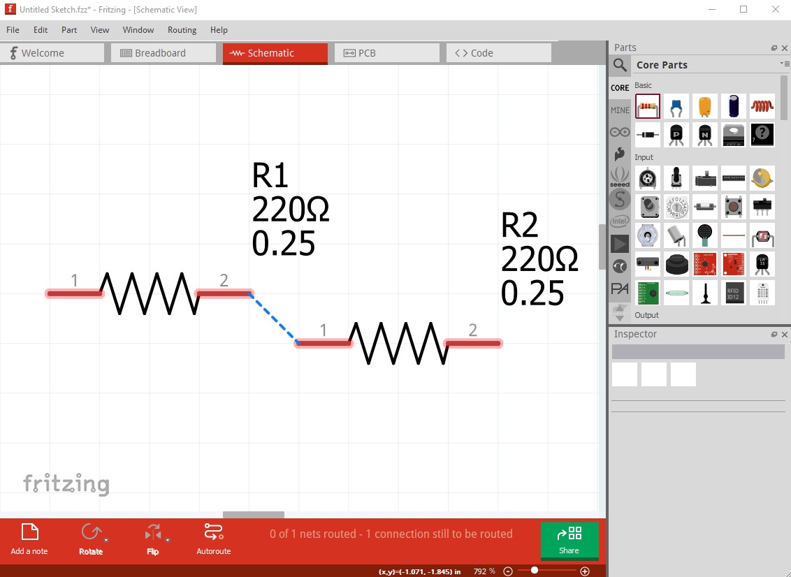
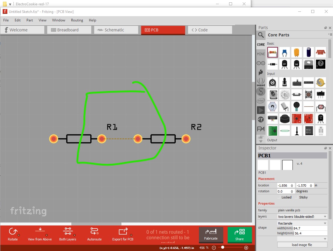
here I clicked on the first pin to make sure all 5 pins in the column light up yellow to indicate they are connected together internally. Repeat for all the columns. Then add a couple of resistors and connect them together to make sure the connections appear in schematic and pcb.

then declare it working as expected. To make the other colors, you need to copy the .fzp and svg file to a new directory then change the names of both files to the new color like this

part.ElectroCookie-blue-17_1.fzp
svg.breadboard.ElectroCookie-blue-17_1_breadboard.svg

then edit the svg and change the board color and edit the .fzp file and change the moduleId, title, property “size”, description and layers image file names to the new values then run it through FritzingCheckPart.py to clean up the Inkscape issues such as px in font-size, then create a new .fzpz file. Changing the number of connectors means adding connector definitions to both the svg and the fzp file for both connectors and buses. Hopefully this is clear enough to allow you to do what you want.

Peter

Awesome, thank you very much! I’ll try to follow the procedure to build the larger board, and post the results here.

This is quite the manual, thank you for writing all that down so quickly!

If I understand correctly, SVGs should meet the following requirements:

  • Units should be set to inches
  • 1 drawing unit should be 1/1000 of an inch
  • The pads should be circles; not actual holes in the background board
  • The pads should have a diameter of 0.048 in, including the stroke. The holes themselves, without the stroke, should be 0.038 in.
  • pads should be labeled “connector#pin”, starting at #=0 in the lower left corner, and increasing count in upward direction before advancing to the next column.
  • The elements that comprise the board should be grouped and the group should be named “breadboardbreadboard”

I’m not certain about the following:

  • Text should NOT be converted to paths, and should be in the OCRA font?
  • Where can I find the “SvgSetConnectorsbb.py” and “FritzingCheckPartw.py” scripts?

Then comes adapting the fzp, which I’ll study next…

  • To work correctly in Fritzing, the svg needs to have real world units (not px «pixels»). For normal breadboard, inches is convenient, because the holes are 0.1 inch apart.
  • 1/1000 inch drawing units is a convention. It makes the holes 100 units apart.
  • The pads need to be an actual graphic element, to be able to have the id / label for the connector. A hole can not have an id. Circles are easy, though technically other graphic elements would work.
  • Their is no fixed sequence required for the connectors. Starting at 0 is strongly recommended, as is counting upward from there. Having a simple pattern makes linking them together in the fzp easier. That has a ‘bus’ section that identifies each group of connectors that are electrically connected together. Using the pattern in Peter’s example means that each bus for the main body of breadboard will be a consecutive group of connector numbers. Typically groups of 5. Any side power rails/busses need to be added as well.
  • Text as paths would work, but using regular text keeps the files smaller. Simpler and smaller graphics files are preferred for performance. OCRA is one of the fonts that Fritzing understands.
  • I believe the scripts are Peter’s custom code to help populate the part files. Placing 300+ connectors manually is slow and error prone. Even with group copy and paste, each of the connector id’s needs to be unique.
1 Like

In general pads should match the pin of the part. In this particular case, it is likely the holes in the board are set for a 0.1in header so I used the standard 0.038in hole size. Usually that would have a 20thou stroke size and thus have a diameter of 0.078in but that is much larger than the pads in your svg so I reduced the stroke width to 5 and the diameter to 0.048in to produce a 0.038 hole. For a normal pad you likely want the 20thou stroke width to give you more room to solder. As noted, because breadboards don’t have pcb, in this case it didn’t matter though any circle size will work fine in this case.

“breadboardbreadboard” is a special layerId only used for breadboards (and some other parts that want to act somewhat like a breadboard such as the Arduinos.) A normal part should have a layerId of “breadboard” for the breadboard svg, “schematic” for the schematic svg and “silkscreen”, “copper1” and “copper0” (with copper0 a child group of copper1) for pcb. Breadboards don’t use either schematic or pcb and thus “breadboardbreadboard” is used for all three here. In practice the layerId names are set in the .fzp file but I think the code sometimes depends on the normal values so using them is usually the best bet.

Either will work, paths for text are recommended where you need a particular font for some reason as Fritzing only supports OCRA and DroidSans fonts and will substitute other fonts in to one of those 2. I find it much easier to change text that isn’t a path when modifying parts and thus try and use one of the supported fonts.

An earlier version of FritzingCheckPart.py is available in github here:

SvgSetConnectorsbb.py was modified to deal with breadboards and isn’t yet in a shape to publish. There is an earlier version in the above github repository as FritzingCreateFzpConnectors.py but it won’t generate the correct template for a breadboard (thus the modification.) I can probably clean it up a bit (mostly, as I was doing it, I ignored the getopt options when making the changes) and post it. It will be useful because it can optionally start at any starting connector number and thus you can just add new connectors to the existing set to get larger. It would be better (and I considered it, but decided to do it manually) to also generate the needed bus definitions at the same time. But that will trip up on things like the power strips of a typical breadboard and needs more thought.

Peter

1 Like

Following the instructions, I was able to create the boards. They passed the test of placing some resistors/wires and seeing if those show up in the schematic and pcb views. I also found it is no problem to put actual holes in the boards.

Maybe it would be even nicer to make these boards variations of the same object? Anyway, this will do. When I find more time, I will move on to creating the larger boards.

Thank you for the help!

Unfortunately I cannot post more than 2 links.
ElectroCookie-black-17.fzpz (7.9 KB)
ElectroCookie-blue-17.fzpz (7.6 KB)

Looks good. I believe the forum will let you post 2 more links in each new reply. I’ll clean up and post the create-cons-bb.py (used the wrong name in the original post) in a bit.

Peter

OK here are the two scripts you need. They both (as does FritzingCheckPart.py) need python 3 with the lxml module loaded. The FritzingCheckPart docs on github have instructions on how I run it (via cygwin on Windows.) This isn’t actually a fzpz file, but rather a zip file of the 2 sctipts so just unzip it and you will get the two scripts.

scripts.fzpz (5.3 KB)

create-cons-bb.py file 8

will create an 8 connector (starting at connector0) block of connectors like this:

<connectors>

output from the script:

  <connector id="connector0" type="female" name="Pin 0">
    <description>breadboard socket</description>
    <views>
      <breadboardView>
        <p svgId="connector0pin" layer="breadboardbreadboard"/>
      </breadboardView>
      <schematicView>
        <p svgId="connector0pin" layer="breadboardbreadboard"/>
      </schematicView>
      <pcbView>
        <p svgId="connector0pin" layer="breadboardbreadboard"/>
      </pcbView>
    </views>
  </connector>
  <connector id="connector1" type="female" name="Pin 1">
    <description>breadboard socket</description>
    <views>
      <breadboardView>
        <p svgId="connector1pin" layer="breadboardbreadboard"/>
      </breadboardView>
      <schematicView>
        <p svgId="connector1pin" layer="breadboardbreadboard"/>
      </schematicView>
      <pcbView>
        <p svgId="connector1pin" layer="breadboardbreadboard"/>
      </pcbView>
    </views>
  </connector>

end of output from the script

</connectors>

doing

create-cons-bb.py file 8 8

will create 8 connectors starting at connector8 which is useful for adding connectors, but probably isn’t useful here as doing

create-cons-bb.py file 16

will produce the same output in a single file (it is useful in the normal script when you have modified the descriptions and need to add more connectors!) The output file is then copied in to the .fzp file to replace the text between

  <connectors>

and

  </connectors>

to set the new connector layout.

SvgSetConnectorsbb.py takes an svg file and starting at the first label with “connector” it finds, renumbers the following drawing elements as connector0pin, increasing the number by 1 for each pin. That means there can’t be any ids starting with connector before the first pin in the svg (and that the pins need to be a the bottom of the svg. It saves the original svg in a file ending in .bak so running

SvgSetConnectorsbb.py test.svg

will create test.svg with the pins renumbered and the original svg file in test.svg.bak (in case of errors!) These two scripts should enable you to make larger breadboards. Note that if the bigger ones include power rails (which I think they do) you will need to create new buses that include all the power rail pins that should connect together in them.

Peter

My python skills are unfortunately very limited, but I believe I understand how the XML is put together and I have created a Matlab script that numbers the connectors and creates buses instead. This seems to have worked as well, as I’ve succesfully created a larger board including power rails.

The only odd thing is that after the board is imported, and dragged into the breadboard view, it takes a long time to actually appear. Is this due to the letters being included as paths instead of text?

Edit: I now built an alternative version with text instead of paths, but it doesn’t make a difference in loading time…

Edit 2: I see I have mixed up the positive and negative rails… and orientation of the brand name… let me fix that…

Updated file:
ElectroCookie-red-30.fzpz (22.9 KB)

What ever scripting language you are comfortable with is fine (especially when it works which it looks to have in this case) :slight_smile: .

That said it looks like translates are biting you:

The layerId breadboardbreadboard is missing (which will make the breadboard not operate quite correctly!), but more important is the transform. Here I ungrouped everything (which removes the transforms)

then did Edit–>Select all and grouped and renamed the group to breadboardbreadboard

which leaves nothing but the initial translate. Now the part loads as expected quickly.

ElectroCookie-red-30-fixed.fzpz (23.9 KB)

so I expect that number of pins being translated causes the load slow down. This is why I usually ungroup then regroup the entire svg as my last step to remove all the translates and avoid performance issues.

Peter

1 Like

Perfect, thank you!

I’ll upload the parts when I’ve made the others as well.

Edit: I’ve found that i need to do ‘select all in all layers’ and then ungroup, and also I had to set the scale to inch. Now I got them to work quickly too.

The sodipodi stuff is Inkscape metadata. You should be able to eliminate that (which again I do automatically) by saving the svg as plain svg like this (File-> Save as then set the file type to plain svg) although for me with Inkscape 1.12 on Win10, the ungroup to remove the transforms fixes most of the load problem. Saving as Inkscape svg may be slightly slower to load, but is no where near the time with the transforms in. I didn’t think that Fritzing paid any attention to the Inkscape metadata, but maybe it does sometimes!

Saving as plain svg in Inkscape is recommended for Fritzing so I do it automatically.

Peter

1 Like

I may have been wrong about the metadata; getting rid of the transforms yielded the biggest improvement!