I created a custom part using Inkscape and a text editor. Everything went great until I ordered PCBs in The Fab. Because The fritzing Fab automatically uses copper fill my PCBs are unusable as all pads got included into the copper fill.
The part with copper fill applied (I can only post one image):
My custom part is here:
kdc_nxj1.fzpz (38.3 KB)
How should I define the pads so that fritzing doesn’t include them into the copper fill? I’ve done other custom parts but I have the problem only with this one. As I cannot find the relevant difference I wanted to ask here what defines if a pad may be included into copper fill.
It might be that the part doesn’t have a copper0 (bottom) layer when you are using THT parts, and that the fill is on the bottom side.
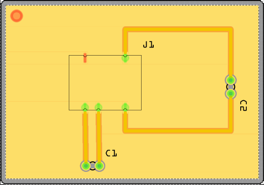
As you might see in the picture it’s not a THT part but an SMD, so it must not have a copper0 layer. But anyway thank you for the answer!
I meant that maybe you have SMD and THT parts on a double sided board, so the copper fill is on the bottom side and not flooding the top. You can see the gaps on the THT parts because the copper fill is on the bottom, but you can’t see gaps on the top side because you are seeing both layers at once…
No sure what is wrong with it but I think it is because it is in millimeters and should be in inches. I replaced pcb.svg re-saved in inches and there appears not to be any problems…
DC Converter-v2.fzpz (38.2 KB)
Your part worked! I tried to use your explanation to modify my version and still had no luck to get it working. By comparing your modified version to mine I found the problem and got my version working too: fritzing isn’t able to handle transform attributes in SVGs correctly. As soon as I removed the transform attributes (calculating the correct coordinates to apply the transform) fritzing was able to handle my SVGs with millimeters too.
Thanks a lot steelgoose for your modified version as it helped me find the true reason for the falsely applied copper fills!
When Fritzing was developed, that was on of the issues… the idiosyncrasies of transform attributes. Inkscape, AI, and CorelDraw are all different. Some transforms work and some don’t work… If you have a through hole connector in the pcb view and it is rotated (transformed), it will have a little red dot in the center… if not transformed it will have a red like halo in the center. I try to stay away from transformed attributes as much as possible… especially on the connectors.