Copper fill area

Can somebody help me in creating a copper fill area which is connected to all the ground connections of my circuit? Is it possible to have a copper fill area on both sides of the pcb?
Thanks in advance

Hi Martin_ge, welcome to the forum!

I was just about to post looking for help on the same subject, so I’ll just post what I have here, and maybe we can find help together.

fritzing has a copper fill and a ground fill options. Copper fill is not connected to anything, it’s just copper area that isn’t removed during pcb manufacture. Ground fill is connected to ground, or some other connection you desire. You could have a ground fill that is actually a 5v supply for example, while it’s called a ground fill, it would only be connected to 5v connections. So I think you are looking for ground fill.

The ground fill options are found in the pcb view’s ‘routing’ menu, under ‘ground fill’ option. To create a ground fill, under the ‘ground fill’ menu, choose the ‘Choose ground Fill Seed(s)…’ option. A popup window will open and you can select what nets you want the fill to be connected to. Once you select what nets you want the fill to be connected to, choose the ‘OK and ground fill’ option from the popup window and a ground fill will be created. The ground fill will be created on the side(s) of the board that are currently active for editing. For example, if only the bottom side of the board is editable, the fill will only be created on the bottom side. If both sides are editable, the ground fill is placed on both sides.

Here’s what I get when I do that on my current project:


I have the ground fill on both sides of the board. My ground ratsnest wires weren’t routed before running the ground fill and they still show up after the ground fill. Most of the ratsnest wires will disappear if I add a bend point to them, but I have a few that still want to route as a trace. I haven’t figured that part out yet.
Also, there are some parts of the fill that are red in color, which I believe mean they aren’t connected to anything. From here on out, I’m not sure what to do, I think I will need to connect the ground fills that are red in color by connecting to other parts of the ground fill with vias, or running traces.

But this is all the further I have gotten on this project so far…
Hope this helps,
Randy

Searching for “ground fill” in the forum search bar will turn up previous discussions on ground fill issues. I’m not sure there is anyone left in the forum that is an expert on ground fills (I haven’t used them so can’t help) so the old posts may be the only help available.

Peter

Ground fill should be done after routing is complete. Otherwise, there may not be a path to connect all of the connectors in the “ground” net. Any remaining routing could need vias, which might require ‘islands’ in the ground fill, or need existing traces to be moved to leave room for the via. Visually the ratsnest line on the middle-left of the uploaded image is such a case. With the fill in place, it is difficult to see traces on both sides of the board, but it appears that the one (interior end) of that ratsnest line is surrounded, so a can not be directly connected to the existing fill. The red sections are filled areas (islands) that do not connect to the ground net. Because there is no (wide enough) path to them from the rest of the fill. Wide enough, because the fill honors whatever keepout limit is configured.

Thanks both microMerlin & vanepp!

I did search the forum and found some useful info.

I hadn’t routed the GND wires, I kinda thought the ground fill would connect them?.. … . :roll_eyes:

With the GND routed, I did a ground fill again:

And now I have ground fill islands, each island has a red dot because it’s not connected to anything. Those red dots were in the previous picture I posted, but I didn’t notice them. Now I assume I need to route connections between the islands?

The red islands will be deleted, they aren’t worth the hassle of connecting them. This is a redesign of a PCB I already had made and used before, and it worked without any ground fills at all.

So adding in ground fills is like icing on the cake…

Thanks,
Randy

You only need to connect the islands if you are “really” set on making them part of the ground fill. Without a connection, they become copper fill, instead of ground fill. Not normally a problem.

I think the red “dots” are the connected ground fill areas. It is the red islands that are are not connected. Usually those are small enough to make adding a connector ‘awkward’. Connecting them would require something like a via, or a jumper. Or sometimes moving a trace to leave enough room to allow a ‘trace’ to reach the rest of the ground fill.

Thanks @microMerlin for your reply.

I have looked into this a bit further and here’s what I am seeing -

First off, I deleted all the islands that were red, too small to be worth the effort.

This is a double sided pcb, but I’m only showing the bottom copper layer:

The red dot marked ‘a’ appears to be a connection to the ground fill for everything outside of the yellow rectangle. All the traces with a gray outline are not ground traces, the ones without a gray outline are the ground traces. Isn’t a red connector an unconnected one? Red connectors everywhere else means N/C. So this is confusing…

The red dot marked ‘b’ is an island that is connected to the GND net through the via right next to it. Yet it is red. If I run a wire from ‘a’ to ‘b’, both of those connectors turn green. So now are they connected? :thinking:

I didn’t really look too closely at the islands inside the yellow rectangle, because I noticed another problem with the one marked ‘c’. That connector is a GND connection and lights up yellow when any part of the GND is clicked on. Yet it’s not connected to the ground fill. The top copper layer isn’t connected either.

If I am misunderstanding something here, please enlighten me, but right now, I’m thinking this area of fritzing needs a bit of work.

I paid for and updated to .0.9.9 because I saw in the release notes that some work was done in this area in an earlier version. So I’m using the latest version and I am happy to donate to the cause.

Since fritzing is more focused towards breadboards and breakout boards, this isn’t much of an issue. Most breakout boards I work with have ground planes, so does a pcb for breakout boards need a ground plane? Probably not. I just thought I would play with it a bit in fritzing…

Thanks,
Randy

Actually it includes some of the ground fill inside the bottom of the yellow rectangle as well. Examining that image, I’ll revise my description of what the red dots (inside a fill area) mean. There is one dot for each contiguous fill area. Whether that area is connected (has a path) to ground or not. So the number of red dots is the number of fill islands. At least one island will include a seed connector. Completely red islands are too small to display the red dot icon.

Yes, a red connector is not wired to anything. There are only so many ways to ‘tag’ things. A red connector is not connected. A red dot in a fill area identifies an island.

In the posted image, the via is shown as green. I do not see the wire from a to b. Working from the image makes analysis of the nets guesswork. The fzz file would be needed. It ‘sounds’ like a trace that appears connected is not actually. Did you run design rules check? Usually, the ‘not really connected’ traces will cause DRC errors, because Fritzing thinks they are part of a separate net, but are too close together.

If it lights yellow, it is part of the same net. However, that could be through an internal connection in the part (a bus). The traces on the board did not connect to it, so the fill did not include it either. Which could be a “good” thing. It can prevent creation of a ground loop. If you really want it connected to the ground fill, you could try including it (the “C” connector) in the list of “ground fill seeds”. I did not try that.

The whole island that “C” points to is isolated in that image. It does not connect to any connectors that I can see. So, in this case, connecting the fill to the pin at “C” would not create a loop.

Thanks for the reply and your help so far, microMerlin.

I have been thinking this thru, and thru, and thru…

In order to KISS (Keep It Simple, Stupid) this I’ve decided to focus on just one small area. The closer and closer I’ve looked at the ground fill, the more I realize how bad it is. Or maybe it’s me not understanding how to use it. And maybe @vanepp could add his opinion when it comes to parts.

I’ve narrowed this down to just the ‘c’ area previously mentioned:


The connector marked ‘c’ is the GND pin on an ESP32, it’s connected to ‘d’. The trace from ‘c’ is routed on the top copper layer, on the ground fill. There is no outline around it to indicate space between it and the ground plane, so it is part of the ground plane. Same thing with ‘d’, it’s a trace on the top ground plane. The two are connected with via’s and a short trace on the bottom copper layer. Yet the ground fill didn’t connect to the pads ‘c’ & ‘d’. See the three blue circles?

They show ground fill connecting to the pins. Yes, there are traces running to each one, because you have to run ground traces before ground fill. Why are some ground fills connecting to ground connectors, and other’s aren’t? Does it have something to do with the parts?

That’s why I mentioned vanepp, is it something about the parts that is causing the ground plane to not connect to them? The ESP32 part (‘c’), I downloaded from the forum. The ‘d’ connection is on a 2.8inch lcd/spi display that I made the part for myself (with help from vanepp). It’s posted somewhere on the forum.

The parts with the blue circles around the good ground connections, 2 of them are fritzing transistors, and the 3rd one is a adafruit product. So now I’m thinking it’s a problem with the parts. The ESP32 and the LCD.

I have 3 electrolytic capacitors in this circuit, all fritzing parts with different values. Two of them have ground fills connected to the ground connectors, like the blue circles example above. The 3rd one is connected to ground by the wire I routed, like ‘c’ and ‘d’ above.

DRC set to ‘professional’ comes back clean, no problems… or so it thinks

I’m open to suggestions. If either microMerlin or vanepp wants to see the file, I can share it with you…

Cheers,
Randy

hmm, no replies?

Well, I worked on this some more, and it has been an experience. I should probably write a tutorial on the subject and post it up for others, but right now, I don’t have the time. Anyway, here’s my understanding of creating ground fills:

  1. Route all the ground connections on the PCB.

  2. Define ‘keep out’ areas as needed. Keep out areas are spots where you don’t want any ground fills and it’s best to define those in the beginning of PCB layout. This way, you know the areas where you want to avoid when routing traces.

  3. From the ‘Routing’ menu, select Ground Fill → Choose Ground Fill Seed(s)… option. A window will open that will allow you to select what connections (nets) you want to be connected to the ground fill. In my case, GND was the only option. Check mark the connection you want to use. There is a button in this window to generate the ground fills. You can also create ground fills from the Routing menu - Ground Fill → Ground Fill (Top and Bottom) option.

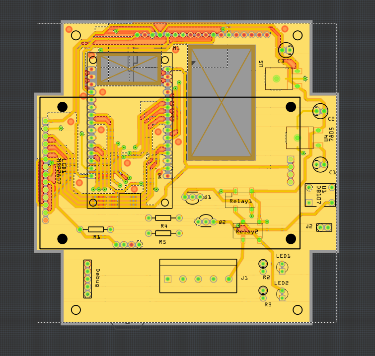
  4. Fritzing will generate the ground fills. This is what I got when finished:


    There are several red islands - in this context, an island is a copper area surrounded by a non copper area. Those red islands are copper areas that are too small to connect to other parts of the ground fill. It’s best to just delete them to clear up what you are looking at.

  5. Once those fills are gone, the remaining ground fill islands will all have red connection dots on them. All those red connection dots need traces routed from them to ground connections on the PCB. Yes, some ground fills will be connected to ground connections with copper, but you still need to connect them so the connection dots turn green. As is the Fritzing way.

  6. After routing the ground fill areas to each other, I was left with 5 islands I couldn’t connect, so I deleted those for clarity. After which, I had this:


    Which looked good to me. Good enough that I ordered 3 PCB from Aisler.

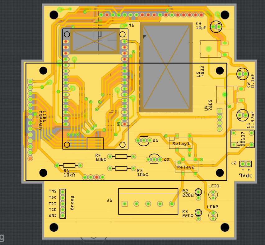
This is the ‘Good’ part of ground fills in Fritzing. I will later add in the ‘Bad’ and the ‘Ugly’ parts of ground fills in Fritzing.

Randy

Now that I’ve mentioned to ‘Good’ parts about ground fills, let’s move on to the ‘Bad’ parts…

In order to create ground fills, the first step is to run traces connecting all the ground connections on your board. Then you select the ground net as the seed for the ground fill and add in the ground fill. At this point, I got to looking around at the PCB and noticed problems with the ground fill. See here:

The three blue circles are electrolytic caps, standard fritzing parts, and all connected to ground. The top and bottom one has ground fills connected to the square pads, the middle one doesn’t have a ground fill connecting it. It only has the routed trace connecting it to the ground fill.

The 2 light blue circles are fritzing transistors and they are connected correctly.
The 2 purple square boxes - one is a 2 pin header, it connected correctly. The other one with 4 pins is a custom part (downloaded from the forum) and it’s connected correctly. 3 other custom parts missed getting nice ground fills connected to them. So some fritzing parts work with ground fills, and some don’t. Some custom parts work with ground fills, and some don’t.

Routing connections to ground fill islands can be a bit challenging. Take this example:

The big green circles are the connections to the ground fill. The little green circles by the big green ones, that your connection point. It’s not on top of the circle as I would expect. This is a minor problem.

At the top of the pic, I have one 16mil trace connecting two ground fills by going between pins of an ESP32 breakout. I clearly have room to run 2 more traces between the pins of the ESP32, but it appears I can only run one trace from connector to connector. Running 3 traces from connector to connector would be better than 1 trace, right? Same thing goes for the lower part of the pic, I could have used 3 traces instead of one.

Another issue I had was the ground fill connectors. Twice, the ground fill connectors were right where I wanted to place a via, making it hard to connect the two together. It would be really nice if one could move the ground fill connector like one does with a components silkscreen label.

At one point, I realized I needed to shift some traces around to connect 2 ground islands together. I moved the traces around, deleted the ground fill, and created a new one using fritzing’s PCB Copper Fill tool. This tool is in the Core part’s PCB View, drag it onto the PCB to fill an area. Drop the top-right corner of the square on the area you want filled. This worked well for that case…

When I deleted a ground fill that covered 3/4 of the board and tried using the Copper Fill tool again, it didn’t work. Not really sure what went wrong there. It just didn’t generate the fill.

Kinda like sticking your fingers in an electrical outlet as a kid. OK, that shocked me, so don’t do it again

Up next, the ‘Ugly’ parts of ground fills,
Randy

If you can document this with an example that is repeatable (and as simple as possible for easier tracing which, isn’t always easy) , it would be good to open an issue on github. The developers may be able to fix the bugs (if they are indeed bugs) if they have an example that recreates the problem dependably.

Peter

@vanepp - Thanks for the advice. I’m aware of the ‘simplest example that shows the bug’ and reporting bugs in FOSS software. I was kinda thinking about writing a tutorial about ground fills since I haven’t found any that show the ‘ins and outs’ of how to do it. However, this circuit board is a re-design of something that already works. I re-did this just to try to address thermal issues, and while I was at it, I decided to play with ground planes. TBH, this project in now in KiCad. I need SMD components instead of breakout boards.

Anyway, on the the ‘Ugly’ part…

After all my ground fill work is done - useless ones deleted, connected ones connected together, etc, etc… I noticed a capacitor’s value was incorrect. So I switched to schematic view to correct the value. In schematic view, I was unable to select the capacitor. See here:

I have the mouse on C1 and can’t select C1. The tool tip says it’s a copper blocker and the tool shelf also says it’s a copper blocker. C2 and C3 can be selected. To make things more interesting, I wnet into breadboard view to fix value of C1. There I could select C1 and change it’s values, but C3 couldn’t be selected and came back as a copper blocker.

Clearly there is a mix up in data in there somewhere.

I’ll try to get something together, but if I don’t, at least there is some mention of it here…

Randy

There is a good chance that the ‘data corruption’ seen is what is causing some of the other issues. It is still a problem, just maybe not where you are seeing the symptoms.