Let’s make things clearer (since Camdenboss is agreeing). I’m doing a Camdenboss board for their CNMB serie.
Here it the specification

The actual state of my part:
 cnmb_c4a9aa2d32a2c11cfd95d0d1f5569774_20.fzp (17.5 KB)
What is done (and checked):
- card dimension
- screw hole positioning
- connector positioning
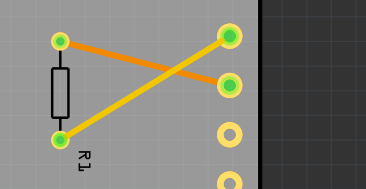
- connection works both sides:
What remains:
- being able to choose the size of the holes
- choose between the two mounting variants (so far I only made the screw one)
- maybe review the dpi by a factor 10
- check part’s rules (color, file structure, …)
- print exclusion area on the board
Actual problems:
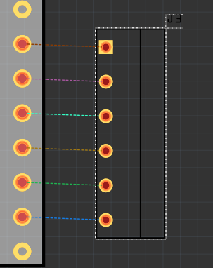
- when I import the pcb svg the link is not made between ui connectors and connectors. Even if I changed them, save, … it doesn’t keep the change. right and left connectors are associated to the same circles
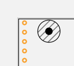
- exclusion area around hole does not display properly. Should be this:
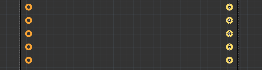
- If I use a connector and tries to put it in the hole on the board, it doesn’t connect:
Question:
- will the connector be drilled by the board maker ?
- will the mounting hole be drilled by the board maker ?
- Is it supported to add parts over the board part ? will this works for a card provider to make the card ?