Newbie needs some help understanding the “Ground Fill” tool in the routing menu. I can’t find any official documentation for this feature.
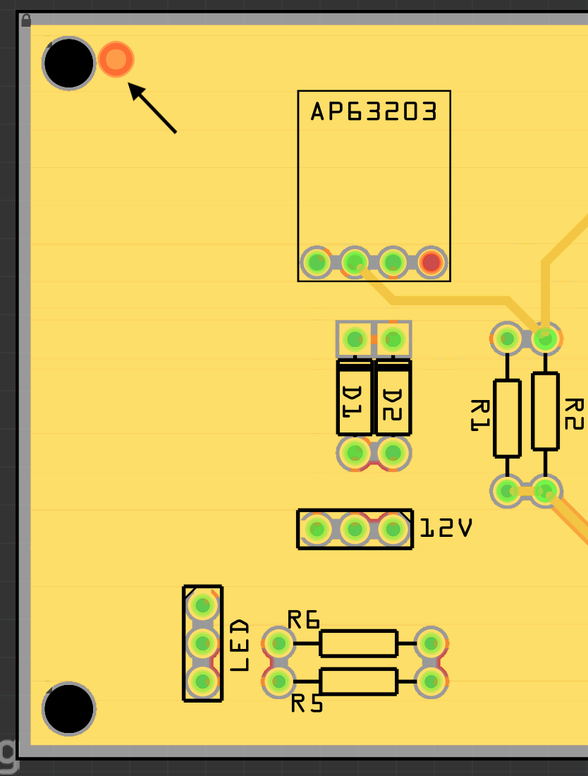
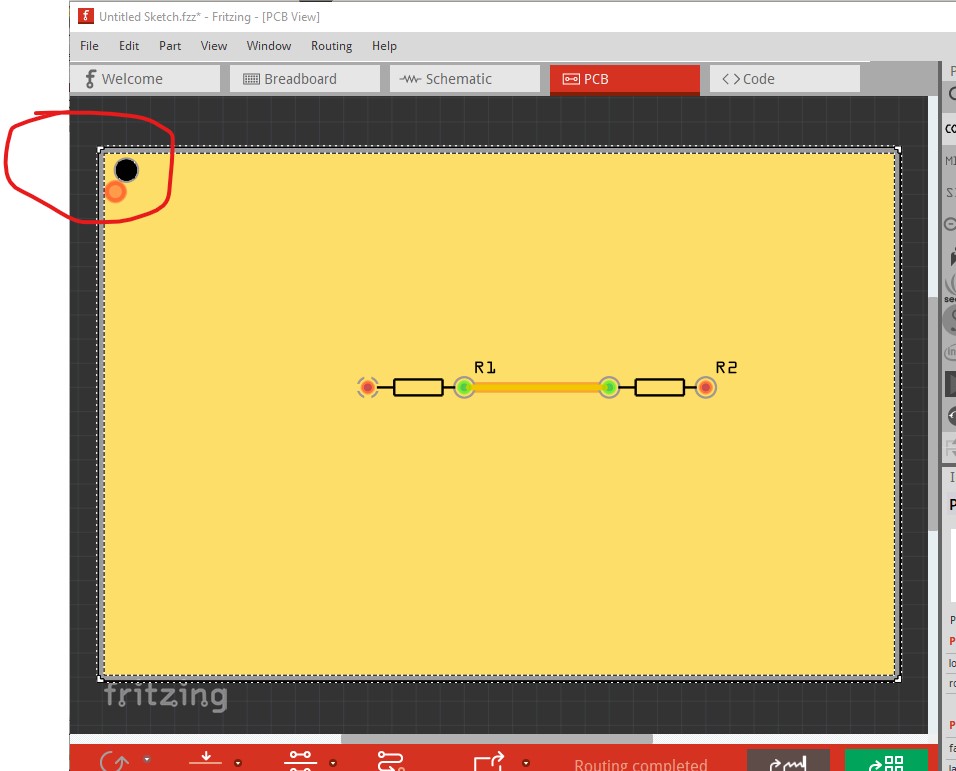
When I was about to send my PCB out for production, Fritzing recommended that it have copper/ground fills. I created a ground fill following some tips I found in other posts on this forum. That’s when I noticed that Fritzing added a new element labeled “connector0: Copper Fill” to the top layer as shown in the picture below. I want to make sure I understand what this is exactly. The default placement is close enough to one of my fastener holes that the screw head will either partially cover it or potentially make contact with it if it’s on the top or bottom layer (as the coloring might suggest). I suppose I can “move” the connector using a a fill blocker, but I’d rather understand what I’m doing first.
Can anyone enlighten me? Does the connector simply join the ground planes of each side of the board, or does it expose the plane(s) externally in a way they might come into contact with foreign objects such as a fastener?