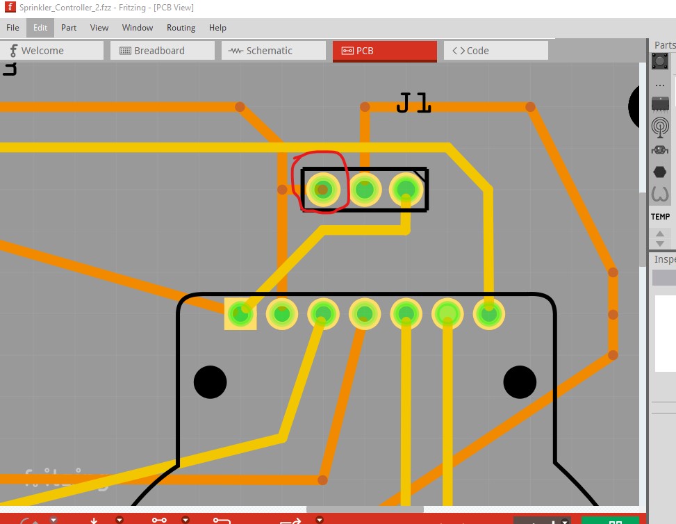
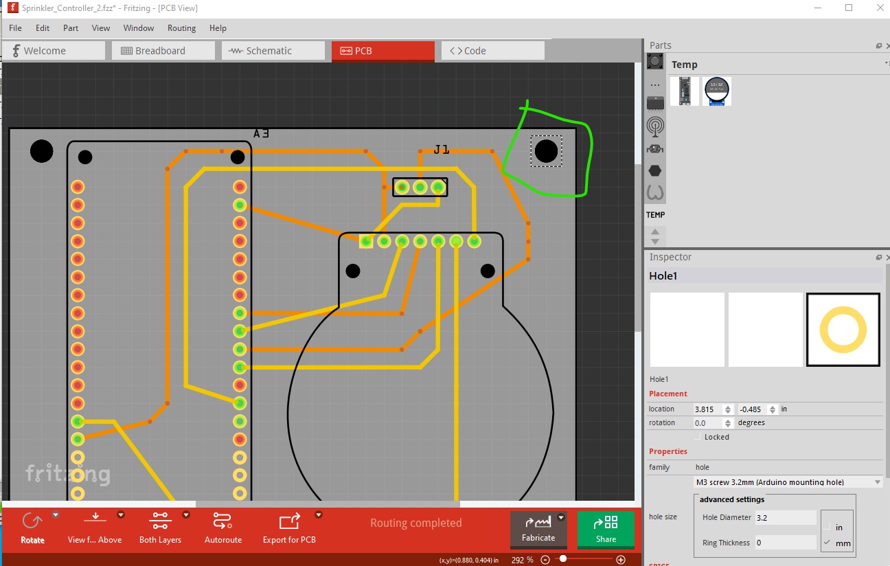
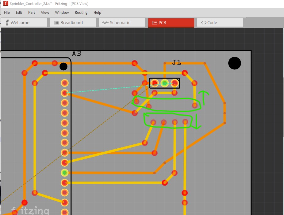
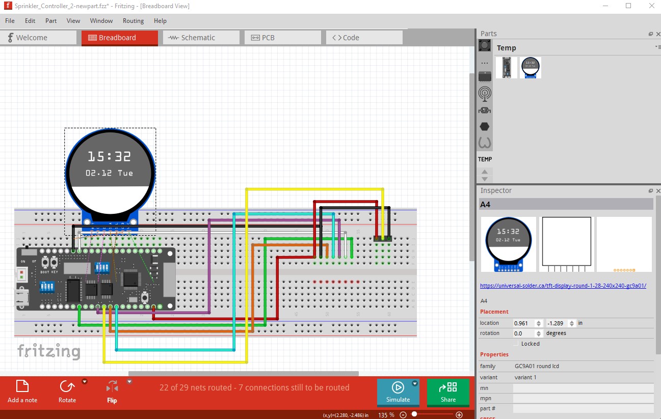
In my PCB layout, after completing all connections, one header hole is orange on one side and green on the other. If I look at the export files, all other hole are circles. This one is a disk. I was concerned that this ment it was a pad on each side and not a thru hole so I re-did the layout and a different header hole now shows as a disk! So, am I misinterpreting the meaning of a disk in the export file? Do I need to (somehow) change this pad into a thru hole and how did I manage to screw it up.
If my question sounds confusing, its because I am confused and its getting late. Can someone have mercy on a beginner and explain this to me?
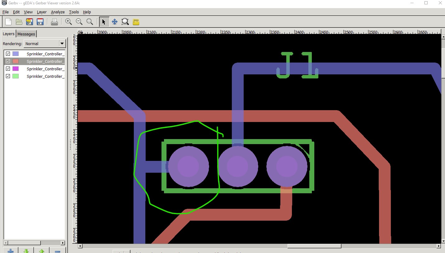
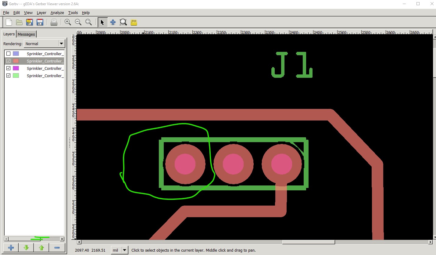
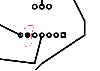
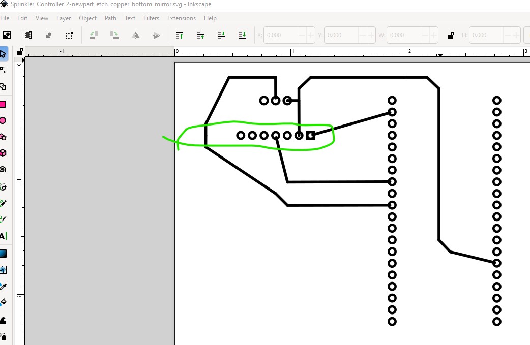
I am assuming you are concerned by the brown spot in the center of this pad (if that isn’t correct you need to tell me what you are concerned about!) I exported the sketch as gerbers and displayed them in gerbv where all looks well
copper bottom, copper top, drill and silkscreen top
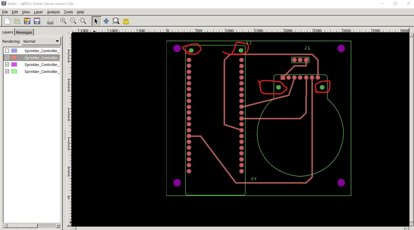
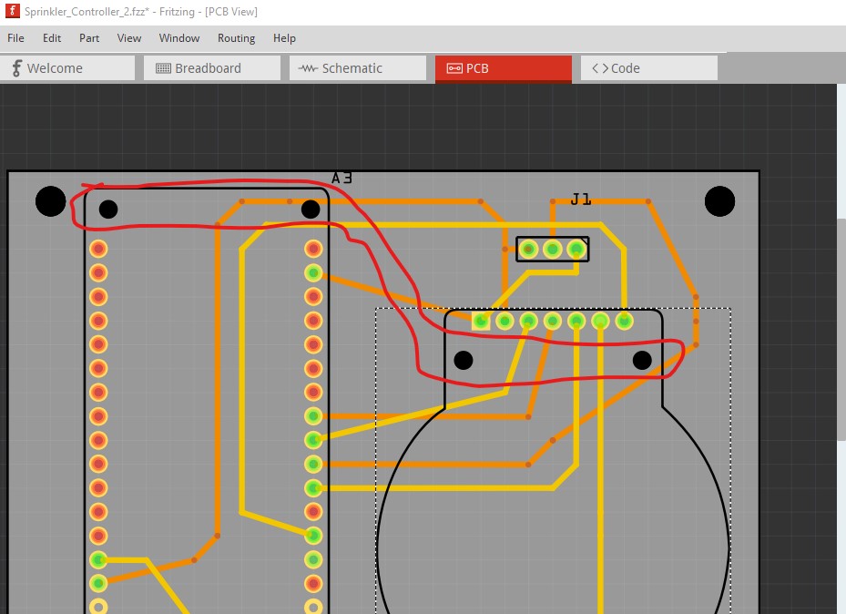
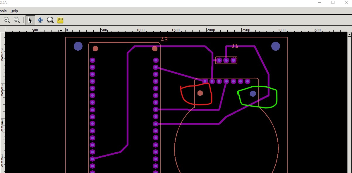
it is drilling a hole in the circled pad and thus all should be well unless I am looking in the wrong place. Note the 4 holes circled in red here are not drilled (which I think is likely your concern).
This is a normal feature of parts. If the hole is drilled in the part you need to change the part to not drill the hole, so the normal practice is to put a hole on silkscreen and tell the user to drag in a hole and place it if they want the mounting hole. The 4 holes in the edges of the board are holes and are drilled.
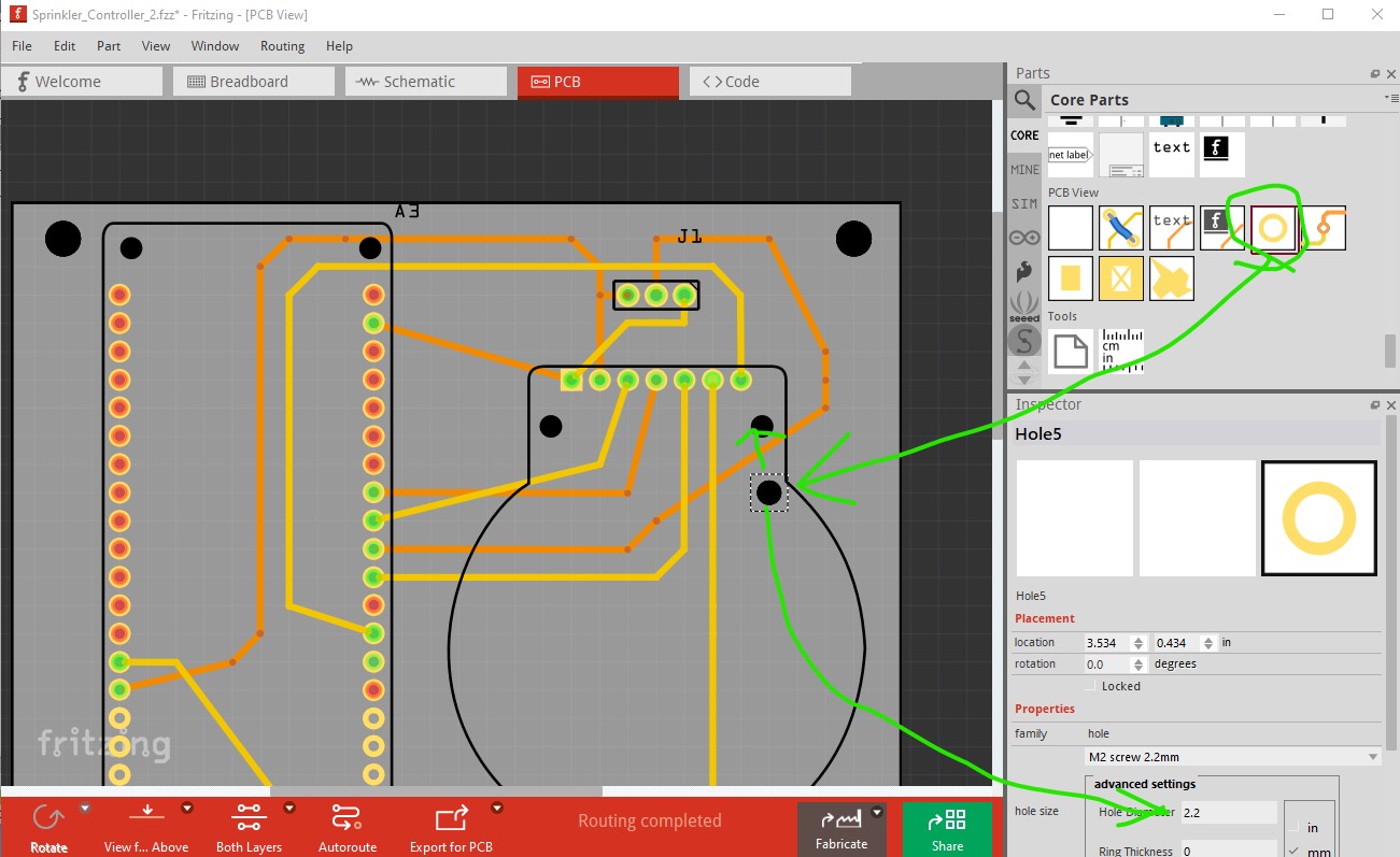
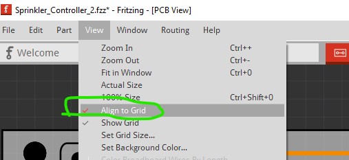
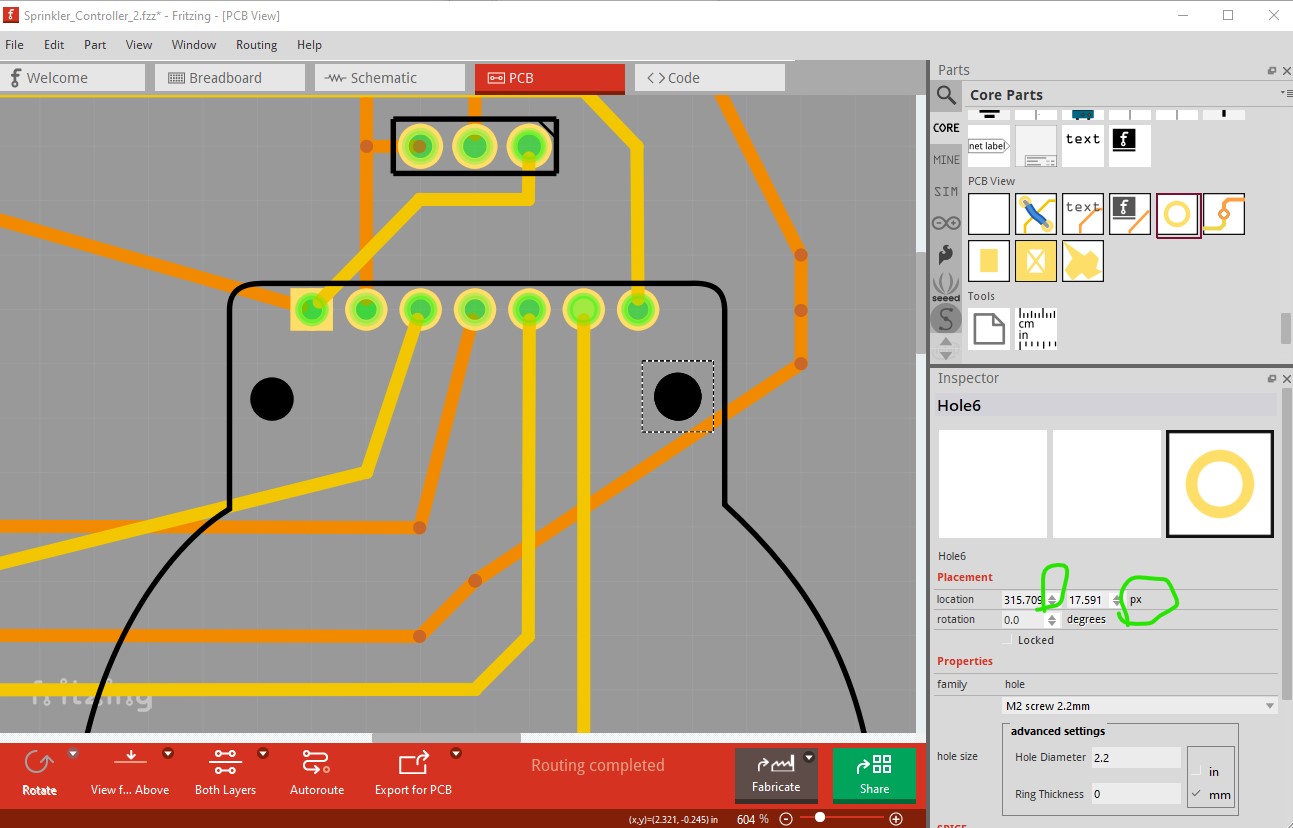
as the holes are not aligned to the grid you can either shut off align to grid by unticking the box in view like this and then moving the hole to the correct place by clicking on it and dragging it like this
or by changing the x/y coords in Inspector. You can type in numbers (if you know them) but probably easiest is to select px (the smallest increment available) and use the up and down arrows to move the hole to the correct position
Wow! Thank you for the detailed reply. Everything you wrote is helpful! I should have been more specific about which hole is a concern. It is the hole , second from the left on the mostly round TFT display. It is not shown with the slightly darker spot in the middle. In the actual layout it is shown as a solid disk. The part did not start out that way it is something I did, unknowling. If you are interested here is thee whole project. GitHub - bill-orange/Sprinkler_Controller: AI application inhubiting sprinklers if rain is coming
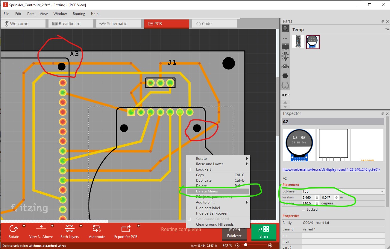
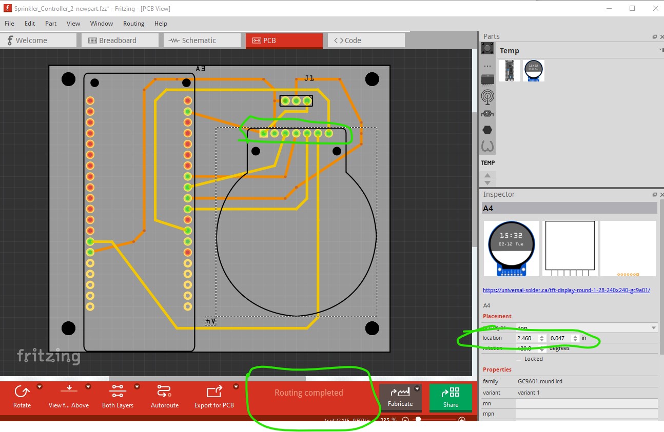
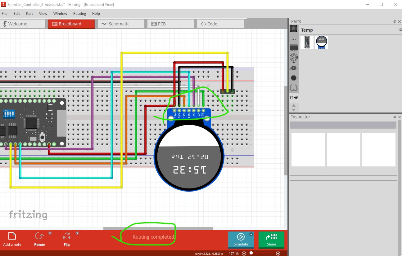
Ah! Turns out this is my fault. There is an error in the part. I just uploaded a corrected part to the original post, so if you download the part again and replace it by doing a delete minus on the current part (which will leave the traces) then load the new part (which will load because of a new moduleId)
then in all views drag the the new part in to position and attache the wires like this. First right click on the display and select delete minus to delete the part but leave the traces. Make note of the xy position of the part in Inspector (the lower right window) so you can place the new part accurately.
then in pcb view move the top traces up a bit and the bottom traces down a bit (this can get complex with overlapping traces though and some times it is easier to just rewire!)
Super! Thank you. My work for now is done. I had a PCB made earlier with numerous mistakes that I fixed with an engraver and jumpers. The project works fine but I noticed some problems. The Dev board I am using has an SD card slot but I accedentially shared its pin with the display, but not the others. Thus, I have a conflict I will just use a different GPIO for that pin. I was planning on using a relay for the sprinkler inhibit, but the current drain to hold the 3v relay closed is pretty high for the Dev Board. I will put an opto-isolator on the board. So, more fun later.
You may want to look at replacing the relay with a power MOSFET. Draw from the Dev board should be smaller (as long as the current is reasonably low, the last person I made a MOSFET for is driving 40A through it …) You probably want to breadboard that before commiting to a new board though but it should be possible and removes the mechanical part of the relay. They make SSR (solid state relay) modules that basically replace the relay. There are a couple with Fritzing parts but making one isn’t a big deal either.