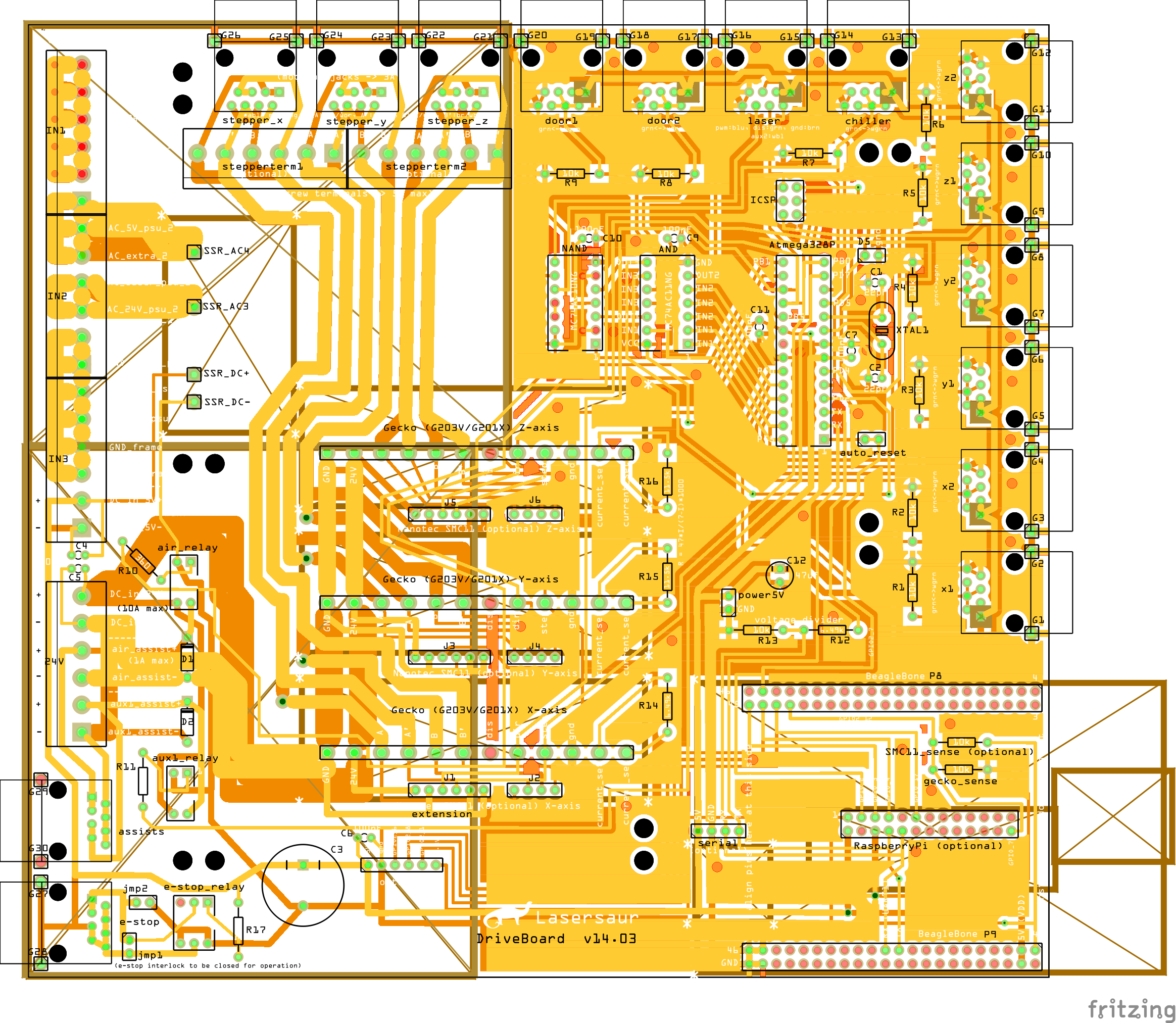
I’ve had some bad news that the project I’m interested in is switching to KiCad, stating that they have out grown FZ, and I remembered a much more complicated FZ PCB posted that I wanted to link to show FZ doing very complicated stuff. The problem is that I have just spent many hours trying to find it but no luck, so I started this post if anyone want to post impressive FZ PCBs we can link.
Nice, but it looks like it’s too late because the guy likes KiCad. They guy said it’s faster, but that is probably due to more parts because I found it slower having to do the same thing multiple of times. Basically you pick parts, lay them out, export the parts, pick footprints for parts you already picked, import parts in another view, and then lay them out. Oh well looks like I’ll have to switch to KC.
Sorry to hear they are making the switch. Maybe you should consider making a fork of it that you maintain on your own. When I first started with PCBs I used Eagle and when I decided to get back into it I found Eagle had been purchased by Autodesk and ruined so I decided I would go with Ki-cad only to find how terrible it was. I tried following a few basic tutorials like a battery and led and switch only to find basic things like SPST switches were not available by default. Then once you found the parts the problem was having to do your project twice (once in schematic and once in PCB) making it very slow. Then I finally decided to try Fritzing despite what I thought of it (breadboard made it look like it was for kids and not a serious EDA). But once I tried Fritzing I was hooked. I was able to work in multiple views allowing me to move components from one board to another in PCB which would move the components from one schematic to another. If it had been Ki-cad I would have to go back and make a new schematic and a new PCB after hoping I knew exactly where every component would sit on my multi-board device.
1 Like
Yeah I know. KC seams like a bunch of separate programs that don’t talk to each other in one wrapper.
I started 2 years ago and learnt FZ because they were using it, but like a month latter they were talking about switching to KC or Eagle so I spent days watching tutorials and trying both. Eagle was out because of it’s 8cm2 limit, and KC seamed so primitive to me. I then spent 6 months of trail and error, because I didn’t know what I was doing and there was no help back then - I hope I didn’t kill this project telling people how to make parts because the FZ crew derived their income from making them -, and made a crude part that swayed them to stay with FZ.
Now I’m back to learning KC, and apart from the trace shove like Altium I don’t see how people are using it with disconnected views. I don’t know all the tricks yet because this is my 1st day, but I deleted a SCH line and in nothing happened in PCB. There must be some trick to it because I don’t want to do everything twice.
After solving problems in this forum about views not matching each other - they were doing it wrong - I now know what to look for and did my 1st .fzz last week using any and every view to make changes, and it was brilliant. You just have to remember each part has a numbered end and not just connect it willy nilly in other views. Also because I kinda know what happens in other views in my head with changes I know what has to be done in each view to keep it correct - if you aren’t sure you just check each view, and by trial and error you see patterns with changes -.
1 Like