Hey everyone i have finished my PCB and taken in some of your input already, I have used the ground fill to make a V+ layer on the top and a V- layer on the bottom if you see any problems with either the PCB layout or electronic circuit please let me know. all the traces are either a on/off signal line with a 10k ohm pull-down resistor or a led line with a 220 ohm resistor or a I2C line with a 4.7 ohm pull-up resistor. also to connect the Mini-360 Dc converter im planning on using a 1x1 male and female header on each corner is that a good idea or is there a better one?
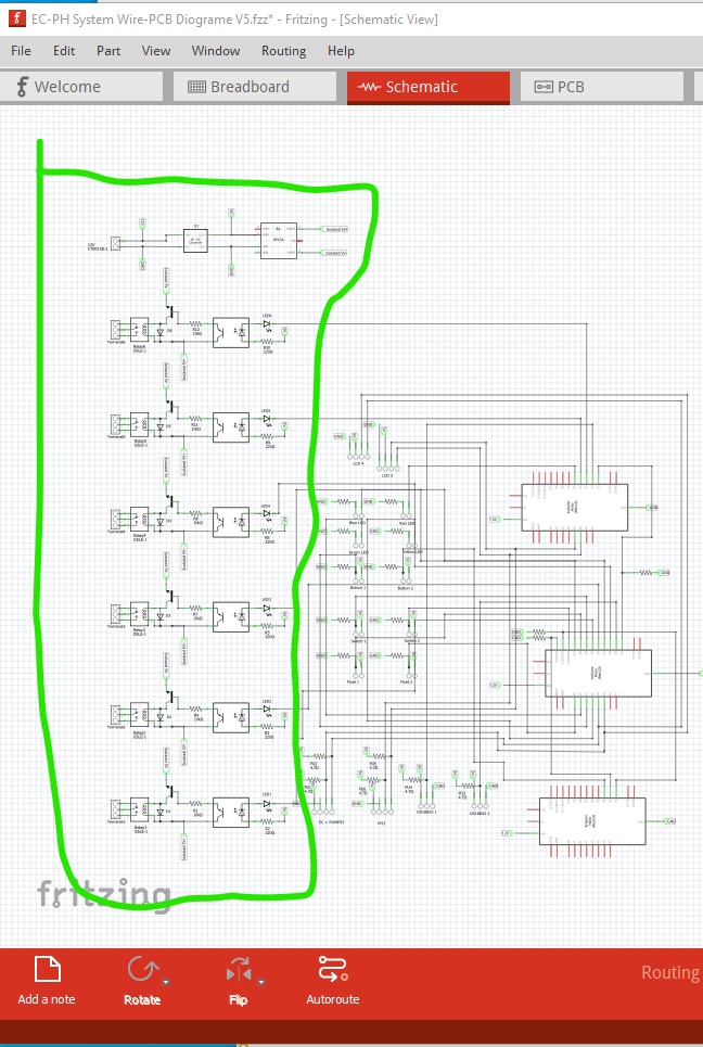
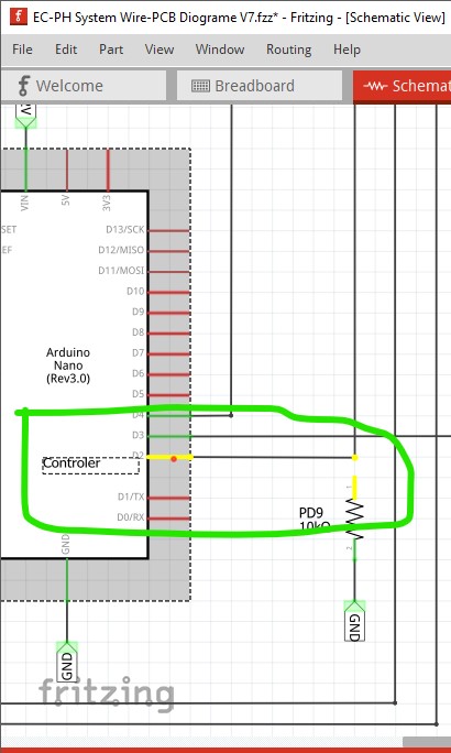
OK, here I started from EC-PH System Wire-PCB Diograme V4.fzz above and made the following changes (there are more to come yet though!) I replaced the relay part with a better one that aligns properly in schematic. In this image I have done a “delete minus” on relay1 which deletes the part but leaves the traces (so you can replace a part without having to rewire) that turns up a problem shown in this image:
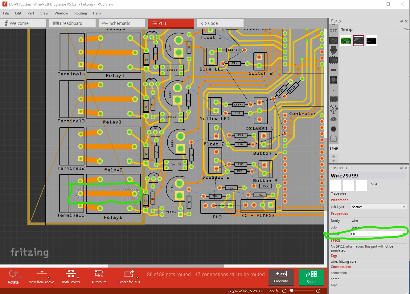
Probably for current carrying reasons you have run traces on both the top and bottom layers and added vias into the traces. Unfortunately it is a bad idea to have two paths to the same place in a pcb (especially on high current paths!) What happens is that uneven voltage drops due to differences in resistance in the traces cause internal current flows in the traces which can cause problems. So I removed all the traces and vias to leave this:
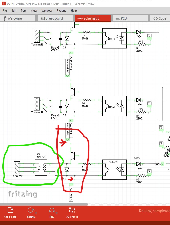
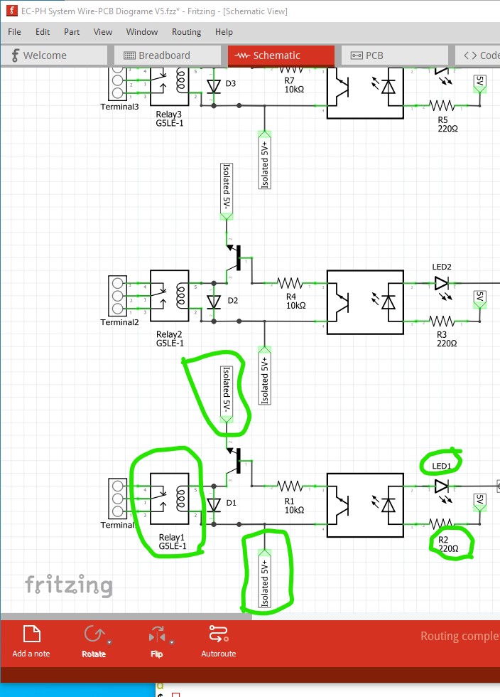
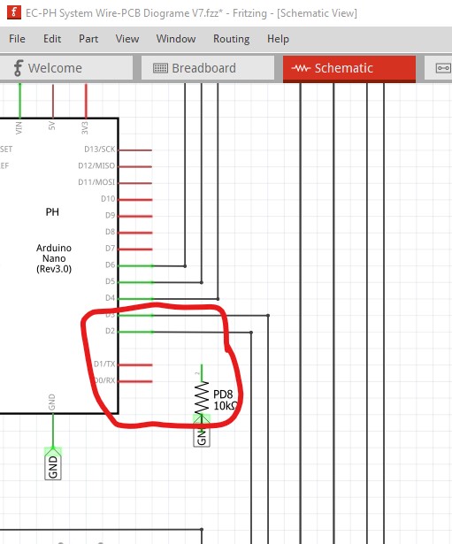
note it has a coil and a box around the relay so it is easy to tell what is contained in the relay. You look to have hit a Fritzing bug with the net labels (I think there is a bug report open on this already) where the connections aren’t shown correctly until they are moved (circled in red here)
There looks to be another bug where you can not scroll down far enough to see the bottom of the net label. I don’t think this one is reported yet, so I will check and report it if it isn’t already (this is Fritzing 0.9.10.)
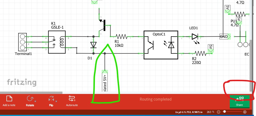
Yet another bug (again I believe reported, but I will make sure) where the terminalId being 0 height or width isn’t recognized as a terminalId which causes the wire to connect to the middle of the pin rather than the end as it should. I will add corrected parts to the sketch to work around that bug. Then I completed all the relays in schematic and pcb like this:
this is a zoomed out image which shows the type of changes I made. The new relay is in place and the various part labels have been moved to make the schematic more readable (circled in green here.) Last is the solution in pcb for the high current traces:
here I selected the wire in Inspector and changed the trace width from the max select able 48mils to 80 mils (almost double the size) by typing 80 over the 48mill entry. You can type in up to a 255mil trace width but larger sizes used to cause a problem and I don’t know if that has been fixed yet. That will basically double the current carrying capacity of the trace (making it equal to the capacity of a trace on top and bottom layers!), and if you need even more, you can specify 2oz copper on the pcb (the standard is 1oz) which would basically double the current carrying capacity again by doubling the thickness of the copper. Here is a copy of the sketch the images came from so you can look over the changes I have made so far.
OK here is the completed sketch. All the nets except ground are routed (I assume ground fill will route ground?) A couple of possible errors in schematic:
the red LED has a three terminal connector, all the others are 2 and there is no connection to the third terminal, was it supposed to be 2 terminals? The pull up resistors are set to 4.7 ohms, I expect that should be 4.7k. I replaced a variety of parts that are broken (including the mini-360) with corrected ones which are included in the sketch. As well I grouped all the connectors in a row so they are easy to find. PCB passes DRC and when ground fill is run should be ready to go. Here is the sketch
Wow this is so neat and much better than mine thank you so much. And yes the 4.7 should be 4.7k resistor, I had a couple question just for general knowledge, for the ground plane should i run it on both sides and connect with vias? also i was curious if it is ok to have 90 degree angels traces I saw somewhere that is bad but wanted to make sure thats true and also are Tee connections ok. and for my future knowledge for making PCB’s should i use a dedicated Vcc trace or is a Vcc ground plane ok?
I’m a bad one to ask because I don’t usually run ground planes, that said I would do it on both sides the more copper to carry the current the better (someone else may have a reason why not though!)
That is recommended best practice, the bends are good for RF and EMI suppression, but for digital traces there is less reason to avoid right angles. Sometimes a right angle is the only thing that will work and in that case it should be OK.
I think T connections are fine (but I’m not an RF or EMI expert and they may not be for that case!)
VCC planes are OK (some fpgas use an entire layer as the VCC plane) but I don’t know if Fritzing supports VCC planes.
A late though, you should check that the ground fill in fact connects all the ground points (or if it doesn’t provides an error message!) I think if there isn’t a clear path to a ground point that meets the DRC rules (sufficient clearance to all other traces it may not connect. Hopefully that causes an error message as routing hasn’t completed but I don’t know if it does (because I have no experience with ground fill.) If the ground plane won’t connect you need to move the traces around until there is a path that you (and therefore ground fill) could route a trace which would pass DRC (Routing->Design rules check will activate DRC) so the pin can be routed by ground fill and I didn’t think to check for that.
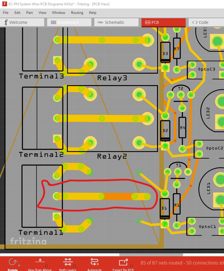
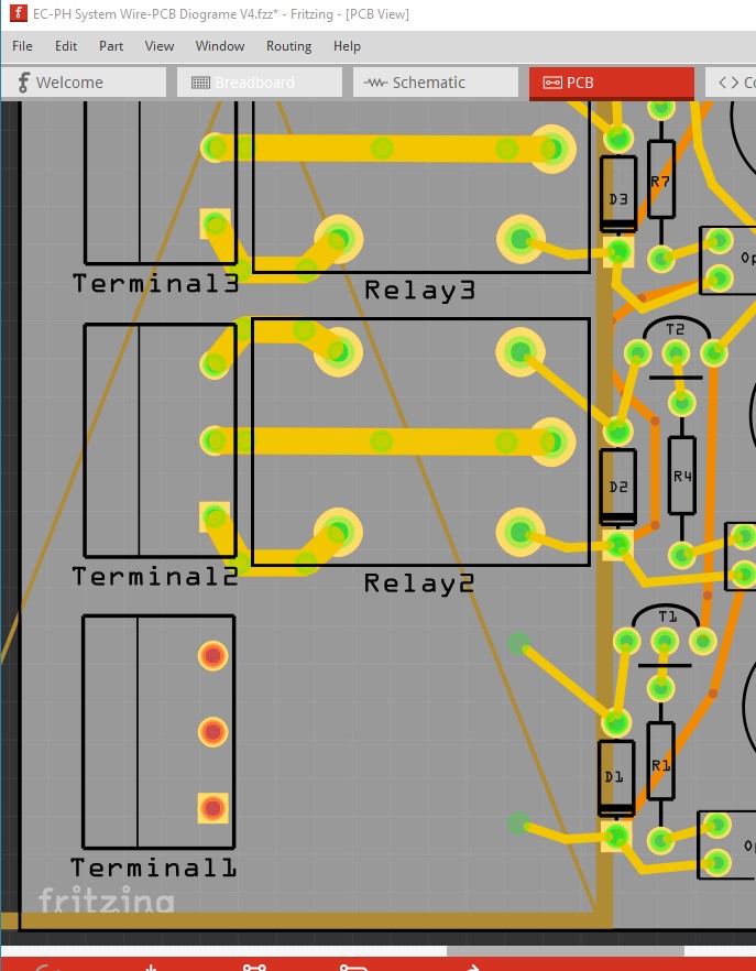
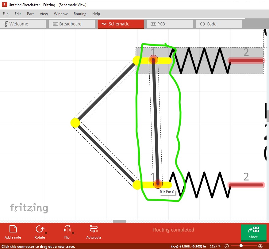
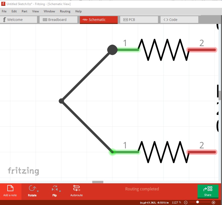
I also see that Fritzing will let you make a loop in pcb where it won’t in schematic:
I don’t think Fritzing should be allowing that second connection as it causes a loop between two components in the form of 2 paths to the same place. It won’t in schematic, if you try the same thing there the second connection won’t connect.
I think the same should be happening in pcb. This also has implications for the ground fill on both sides of the board as if that creates duplicate paths to one or more connections (i.e. one on the top layer and another on the bottom layer) that is undesirable due to creating loops (as do vias between the ground planes which will cause the same issue!)
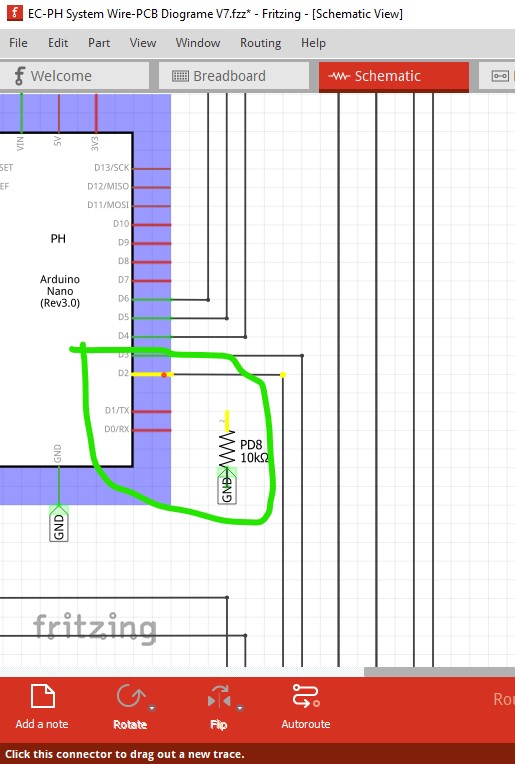
I corrected this by deleting both wires and reconnecting them. That appears to have made the render operate correctly. I thought that I had seen an open trouble ticket on this, but when I checked this morning on github the issue is with the label text not the connection which set me to looking at it again. Now I just need to figure out what I did to cause the problem (because it indicates a Fritzing bug!) so we can fix it. In any case here is a new version of the sketch with that fixed and the other pull up resistors with their value changed from 4.7ohms to 4.7k.
Hello everyone this is my finished PCB I have used EC-PH System Wire-PCB Diograme V8.fzz from Peter and modified it a little bit, then I used ground fill on the top layer only to make all the connections, for 2 Arduino’s I ran a bottom trace to a via to connect it to the top layer, I added the via after ground fill because it would not connect i tried to added the via as a ground fill seed then selected the seed but it would still leave a no fill radius around it. I am hoping the via will actually connect to the top plane. if you have any advice still id love to hear it.
Looks good! All the grounds look to have connected (by clicking on a pin in the net all the pins in the net light up yellow and a visual inspection indicates all the grounds have a connection!)
I have filed one bug report on the resistors not rendering properly (where clicking to straighten a line disconnects the resistor) and I’m hoping to be able to (but haven’t so far) recreate the missing connection to report that too. Since I did it all (your V5 is correct, my V6 is wrong) I should be able to recreate it but haven’t so far. I think this is a bug I have been chasing for more than 5 years now and never been able to recreate (but previous versions have been broken by other people, this is the first one I have done if I can just figure out what I did .)
ok sounds good and is there any thing i should consider when exporting to get it printed? if i understand it right i just download it as a gerber and upload that gerber to the PCB printing website I am planning on using digikey and getting my parts at the same time, also the resistors on digikey have power rating im not sure what power rating to pick as i just used resistors from the arduino starter kit the ohms where like 220, 4.7k and 10k
putting all of those in the zip file usually works (I haven’t used digikey though.) For the resistors 1/4 watt 5% tolerance through-hole should be what you want that is what is commonly used in the starter kits and what the pcb layout is set for.