Here is an Interesting Problem I was wondering if Anyone else has encountered this . I have build several designs in fritzing . I click on Exsport - For Production - Extended Gerber ( RS 274X)… It then goes through the usual file keeping on my computer ,Then I use winzip to make it a zip file , then I upload those files to Fritzing for Manufacturing. When I look at hem on my project page they look really good Everything is there ,… " Until i send them for Manufacturing " After I do That I find traces Missing . And I try to fix it by redoing the Files and uploading it again But They go into Production and I got it back and the traces are Not there Which Means My boards are Trash …
Anyone have that happen ? And how Do I fix the Program ? Is it on my side your Fritzing side ? I have sent Screenshots
Since I rarely make boards I may be of limited help here but that said a couple of things to try. Use a package such as gerbv (from the geda project) or another gerber viewer to look at the exported gerber files before sending them for fab (you should be doing this anyway to avoid just this problem). Sometimes Fritzing screws up for various reasons (see the recent post about missing pads in a smd part for one example) that will show up in the gerbers in a gerber viewer. If the gerber viewer output looks correct then the problem is in either the upload process or at the fab not in Fritzing because the gerber is what the fab will use to make the board. The other thing to do is upload the fzz file for the board that screwed up above (upload is the 7th icon from the left on the reply tool bar). With that one of us can look at what is happening and perhaps tell you why it is happening.
Peter
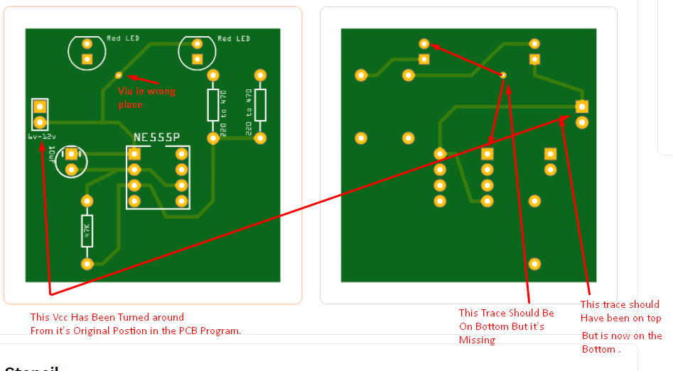
I do not believe the changes that are being made would be a problem but rather they make it better by eliminating the need for any vias (although they did not delete the via) by putting the traces on the correct sides. I guess the reason to turn the 2 pin header around is to make the polarity correct with the LEDs. In the end if you follow the traces it has all the same connections and would have the same schematic.
My guess is this is being done manually by a technician to get you working boards and could be how they justify the price they charge. I haven’t ever used Ailser for production so I can not say they do this for sure. The places I uses that are %5 of the price do electronic testing and inform you if they find anything that is unproducible but they do not evaluate your design for errors.
Is the sketch .fzz correct, like did you force a pin #/polarity swap in one view - upload might show it -, and did you do a design rule check. If you click pin #1 on the 555 does the LED pin turn yellow.
There os an online GerbLook also.
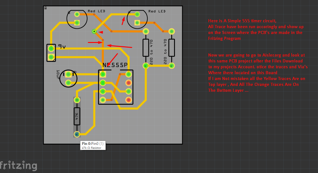
You don’t actually need that via because you can run that trace under the resistors and around the side-top.