Hopefully I have managed to create the “family” grouping correctly. With the SMD parts, I have changed the “type” attribute from “male” to “pad” for the connectors within the .fzp files.
They should actually be male. I don’t know what pad is supposed to do (if anything) although I haven’t looked at the source. The two common ones are male and female. Female is used on the breadboards (and on things like Arduino ICSP pins that would short out if connected to the breadboard), and the rule is female connects to male (i.e. a male part to the female breadboard) and a wire connects either (male male and female female will not connect without a wire.) It is possible pad is used for something I don’t know about (because it appears in some parts in core), but it may also be that anything not male is considered female. Well it appears I am wrong here, possibly anything not female is considered male (or pad really does have some meaning) as your part appears to work fine:
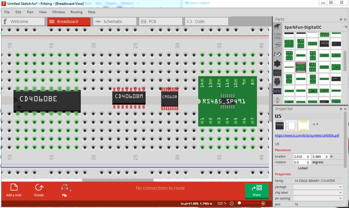
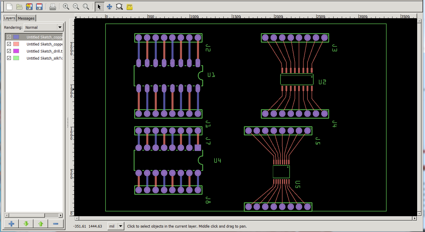
The green pins indicates a connection on the breadboard. Guess I need to scan the source and look for “pad” as a description to figure out what it does (if anything.) For the two SMD chips, in breadboard they are typically put on proto boards (like the Sparkfun chip on the right) to allow connections on .1 boundaries. I usually steal one of the Sparkfun chip’s breadboard to do this. The gerber output looks fine:
The default DRC rules are unhappy with the soic package but that is fairly standard and would probably clear with more relaxed DRC settings. The family and variant stuff looks pretty good, a few suggestions though:
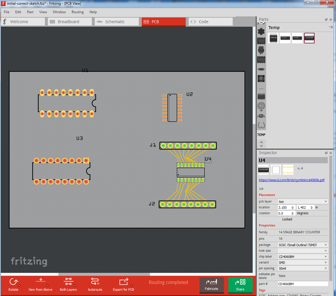
the variant field tells us the pcb pads are oblong. For the standard outline one I’d suggest adding a variant of something like “Standard round pads” to differentiate the pad difference, currently the variant is showing as blank (presumably because there isn’t one)
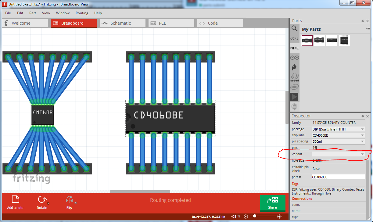
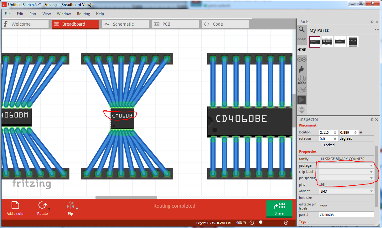
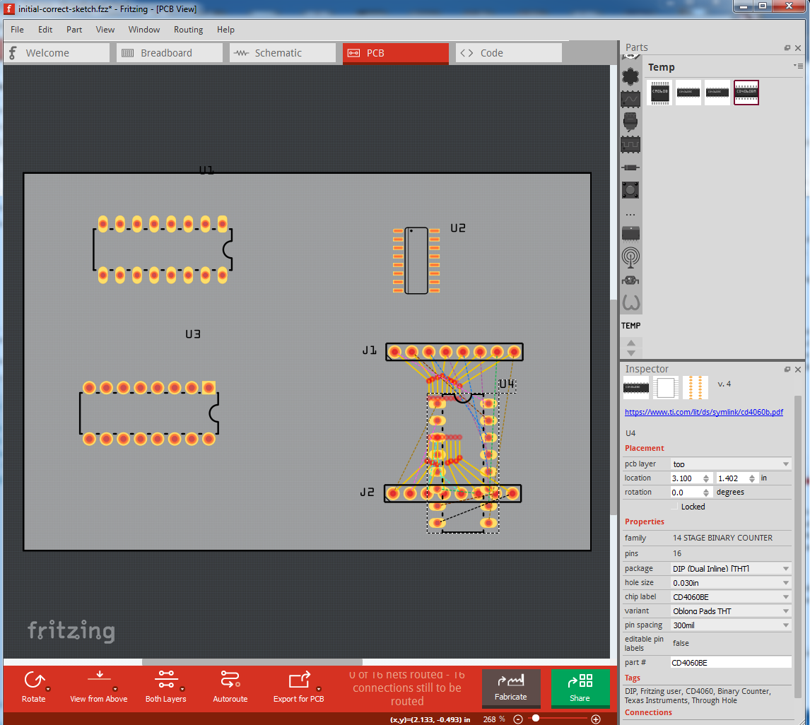
the chip label has been truncated (a smaller font size may help here) and the variant fields in Inspector on the right are blank likely because the property fields are missing in this fzp file. Adding those in so we see what package this is would help. On the way by I found some new bugs as well , I accidentally changed the small outline to one of the dips, when I changed back the traces did not restore correctly (and will not as far as I can see)
It looks like the last bend point is no longer rendering and at least two pins have lost their traces (but not necessarily the connection) entirely (possibly because they are the two single segment, no bends traces.) Assuming I can reproduce this I’ll report it as a bug. Over all a great job!
This is great news! It’s good to have high praise like this, you are an inspiration to all of us and your guidance is always appreciated.
Yeah, I was in a bit of a quandary with the whole “pad” vs “male” thing after reading about it in the GitHub Fritzing/Fritzing-App 2.1 - Part file format - Through-hole vs. SMD parts section, so I decided to go with “pad” for the SMD parts (do you think I should change the “pad” to “male” in the files). Secondly, do you think I should redesign the SMD parts to be on “proto boards” instead for the ease of breadboard layout/connectivity? As you would know that the current SMD part designs are represented as “real life” soldered components on a PCB.
With the DRC, yes I found the exact same problems until I changed the Autorouter “keepout” to 0.005" instead of the default 0.010". Everything was okay then (well for SMD anyway).
I’m a bit confused with the blank fields in the standard round pads THT part as the attributes are in the .fzp (take a look). They appear in my version of Fritzing…Wierd?
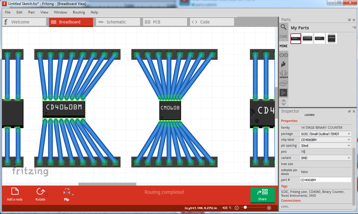
Again the same issue with the TSSOP SMD, I’m a bit confused with the blank fields, as the attributes are in the .fzp (take a look). As for the chip label this is not truncated and is the correct name, CM060B, as this is the official designation for the IC from the datasheet, not CD4060B as you would expect.
I can’t explain what is going on with the traces and bend points issues, I shall leave that to your vast expertise.
Once again I thank you so much for all of your help. I will post the updated parts once modified.
That is probably a good bet until I find out what if anything pad is supposed to do in the type field. The pad looks to be working, in that the parts connect to the breadboard, so either way should be fine.
That is typically the most useful and what has usually been done. As you see in breadboard the wires are big and connecting to fine grained pins such as SMD (and 2mm and 1.27mm headers) is a pain as the wire wants to snap to a .1 boundary but it can be done and either way should be fine. This is a grey area that has in the past been left to the part maker to decide, I don’t know of any documented opinion of the “correct” way to do it. Generally breadboard should reflect real life, but that is sometimes painful when the parts get small.
there is a currently open issue on DRC having troubles with copper (and I have run in to problems with translates confusing DRC sometimes), but I think it is mostly the default rules are not aimed at people doing fine SMD work (they are assumed to be able to adjust DRC .)
I’ll clear my user directories, it is possible that I have something corrupted in them from doing odd things, and I didn’t think to try that, so it may be a problem on my end if it isn’t happening to you.
Ah! I never even considered that :-), I assumed Fritzing had done something odd (although it doesn’t usually truncate text, just runs it over the end of the part.)
Edit:
Yep, looks like corrupted user directories, I cleared them and all 4 parts now load correctly and display the correct things (well mostly anyway, the standard pads version is reporting a 0.038 hole size when gerber is using 0.30 as it should I think) in Inspector. I’ll try and reproduce the change the package breaks the back out of the change and see if that was corruption (or possible the cause of the corruption.)
edit2:
There is a rendering bug, but the Inspector oddities have not come back so that must have been something I did. Starting from here:
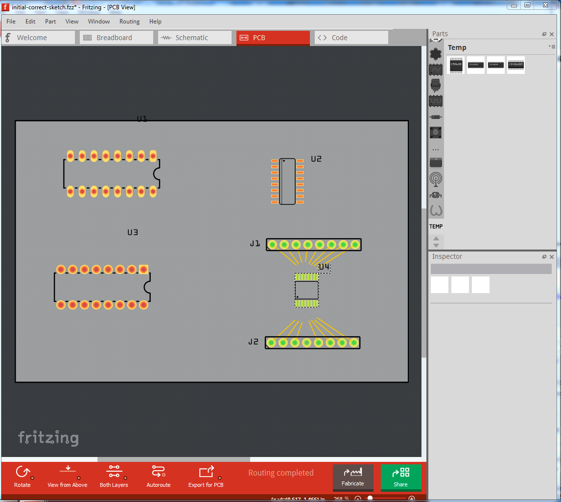
I think the traces should have moved to the pads as they did from tsop to soic not this mess with rats nest lines and unconnected traces. Its possible that SMD to through hole isn’t supported in the swap mechanism though. Now hitting edit->undo hits a render bug:
the last (or in two case only) segment doesn’t get rendered. It is still there, if you click on a header pin the IC pin lights yellow indicating a connection. When I saved this sketch, and closed Fritzing then reloaded the sketch the traces are rendered correctly again. I’ll try this again with the smd chip rotated 90 degrees so its alignment is the same as the THT one and see if that helps. Nope, this appears to be a bug. The interesting thing is that the connections are still live, despite the rats nest lines. If I click on a header pin the correct pin in the DIP IC lights even though the trace is not correctly rendered and there is a rats nest line present (which will cause a second connection if clicked on.)