Hello everyone.
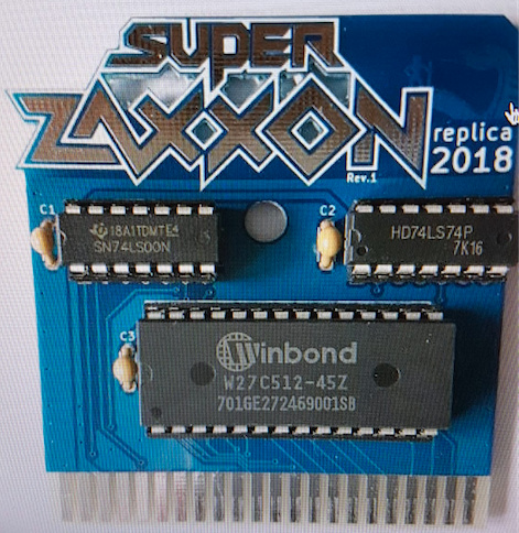
I’d like to ask for advice. I’m making a custom cartridge with a slightly out of the ordinary design. The goal, one day, is to get to the attached design (just for fun). How can I make an inscription (Super Zaxxon) like the one attached?
It would seem to be made like a pad. How can i reach this effect?
Thanks in advance
Dani.
If when you say
I assume you mean it is a pad in the copper. In that case you would need to add such a pad to the pcb svg copper1/copper0 group and it will appear as copper with no solder mask over it. More of a problem is likely to be the edge connector assuming it is double sided. Fritzing has poor support for dual sided edge connectors although it is possible to do it.
Peter
Peter,
thanks for the quick replay. This time i don’t understand. 

Could you make please a quick example (a little file .fzz and/or .svg) ? It seems complicated.
Thanks in advance.
Dani.
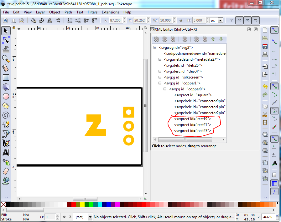
Sure, here is an example part. Note in this the Z is on both the top and bottom of the pcb. It is possible (but more complex) to have it only on the top, but if you need edge connectors on both sides of the board, you have to do that anyway.
pcb svg (available in the part) with a Z made of rectangles (you probably want to use paths.)
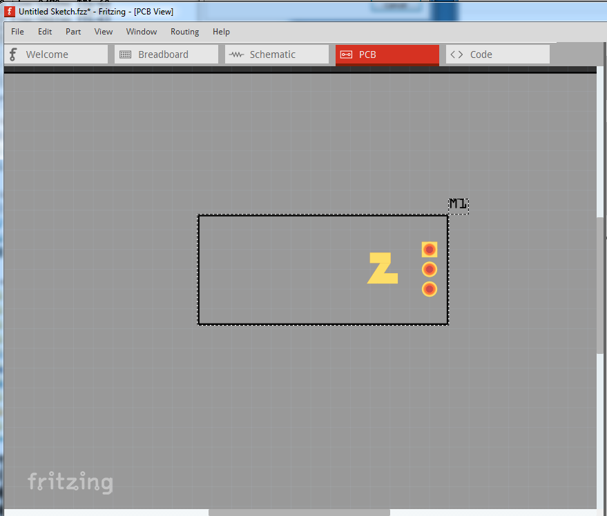
Fritzing pcb view:
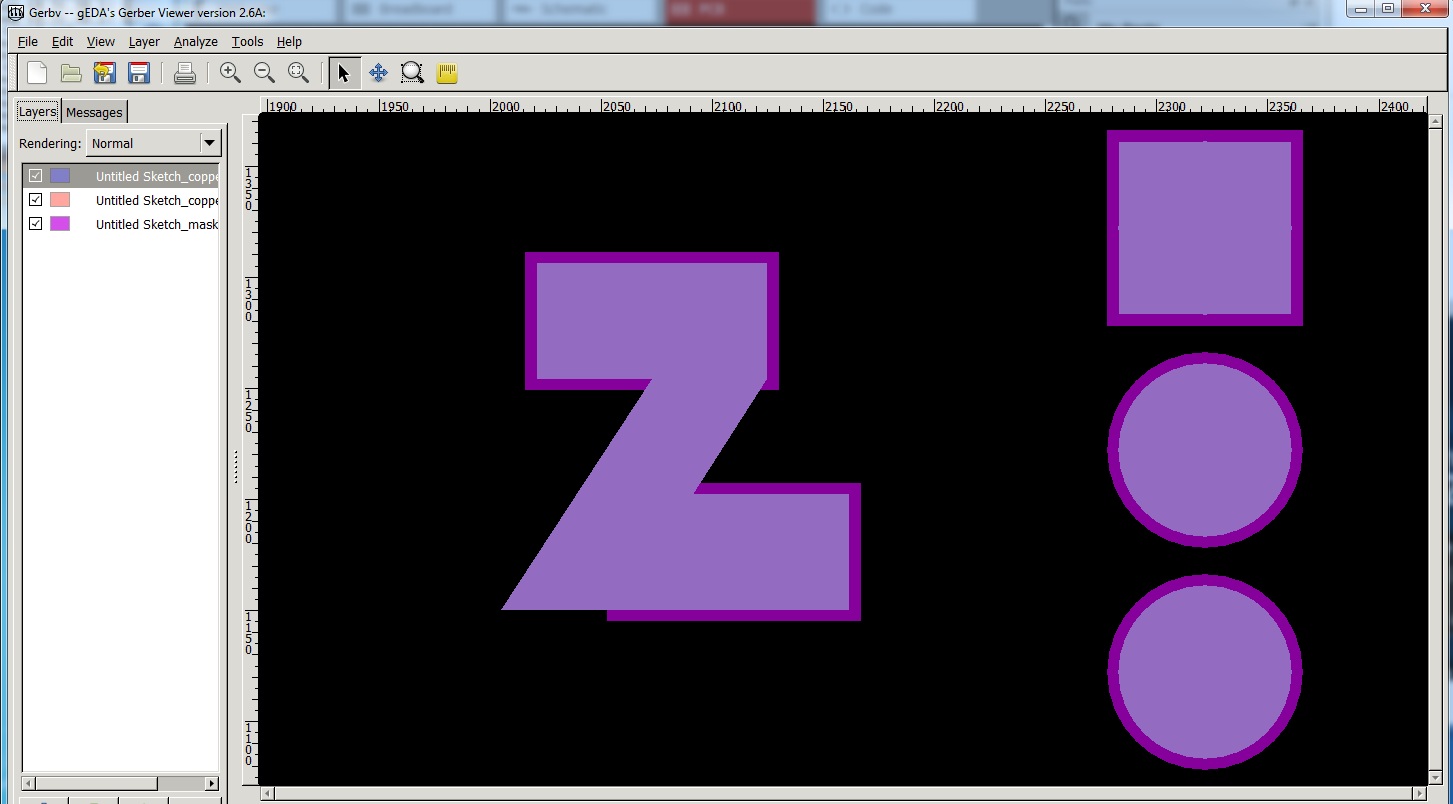
gerber output via gerbv:
The mask layer is a bit odd (the purple lines), but the Z should show as copper. Finally the part that created this:
copper-test.fzpz (21.7 KB)
Peter
Peter,
as always, thanks for the quick reply. I did not understand one thing well. Can it be done only on components? I wanted to do it on a personalized board. I am attaching my board and asking if you can help me out. I tried to add the layer “copper0 and copper1” but unfortunately nothing works.
Usually I draw the board in SVG and then I do the “load image” from Fritzing. Could you help me in adding this copper layers?
Thanks

Sorry for the late reply, my internet connection is having difficulties.
AFAIK you can’t load copper layers, only board outline to add slots and silkscreen. The only way I know to get an image on the copper is via the pcb svg of a part (there may be one, I just don’t know of it). You can move the boardoutline path in to copper1 of the part I uploaded and it will appear as copper (if you do it in copper1 only with copper0 below the path it will appear only on the top of the board as well) probably without the holes as the gerber code won’t recognize holes in a path so you would need to replace them with three circles of the appropriate size and position. If you don’t want plating through, there is an option for that (I don’t remember the keyword off the top of my head but it is in the part file format document near the end.)
Peter
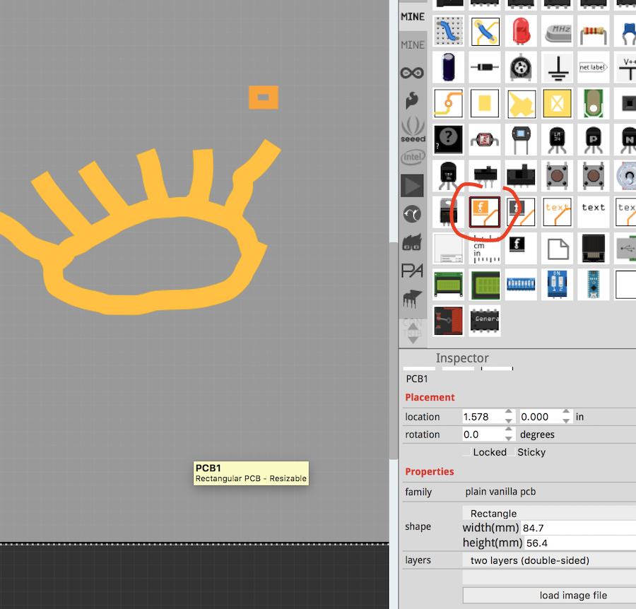
You can add an SVG image of what you want using the part called “Copper Image”.
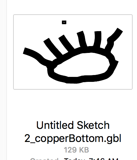
Below shows two items added to copper bottom layer - a rectangle pad and crude ‘eye’ looking shape. Along with the exported copper bottom layer.
If also wanting an image on the Silkscreen, use the Silkscreen Image part…
Thanks! Learned something new again. On Windows that doesn’t show up unless I do a search for it in core parts (and since I didn’t know it existed, I didn’t do that  )! I see it is in your mine parts bin, so presumably you found it and loaded it for easier access.
Peter
Yes, it’s in my parts bin.
When I first started using Fritzing, I searched for all the parts I normally use in projects and created the parts not in fritzing. I prefer using my homemade parts but there are some parts (if want to call them that) such as the copper Image that are must-have’s for my projects.
To address any thoughts of an Error, regarding the position of the Pad shown in Gerber, I moved it before taking the screenshot…