Camdenboss CNMB6 box PCB

Hi,

I made these parts for camdenboss cnmb6 and started for the cnmb9 boxes. I haven’t produced PCB to confirm there are no bugs.
This should help to use these boxes and have connectors aligned with holes in the box body.

There are 2 packages (one for CNMB6 and one for CNMB9) and 5 variants for the board options.

I need here to finalize connectors dimensions, help or advices to put the right dimensions to copper elements (holes, pad, …) are very well appreciated. Other advices comments … are also welcome.

Camdenboss.fzbz (55.7 KB)

These seems to need some work yet to be usable.

I ran the first of those, the cmnb6-a-base, through FritzingCheckPart. I did not check in detail, but here are some highlights.

terminalId entries are in the the fzp definitions for schematic view, but the matching id values are not in the svg file. With the schematic image as is, the terminal Ids are not needed. However, the schematic images are very non-standard. They have circular connectors like breadboard and pcb. Schematic is normally created with 0.1 connector inch lines extending out from the body of the part, and not using the green background for the body. In that format, the terminal id elements should exist, and should be at the outer end of the matching connector line.

Schematic is a “logical” representation. It does not care about things like mounting holes, row spacing, connector pin hole and copper size.

There are duplicate connector«number»pin elements in the pcb. Quick guess: you have separate copper0 and copper1 groups, with a copy of the connectors in each. Instead, the copper0 layer (group) should be inside the copper1 group, and the connectors only inside the copper0 group. Since copper0 is inside copper1, a single connector element is then in both copper groups.

The B, C, D variants load as blank blocks, without any connectors at all. Is that intended?

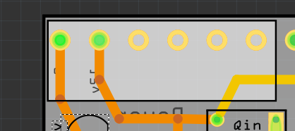
DIN-9, A/Base breadboard has more pins shown than schematic or PCB, but right side bottom 2 blocks of pins are not active. They are just part of the image, without any functionality. For screw terminal, the PCB seems to have the extra pins active, but not breadboard, and they do not exist at all in schematic.

Thanks a lot (again) for these valuable feedbacks. The tool will definitely help. I look at your comments in details and will run the checkpart.

For the BCD boards, these one are plain. I may add some exclusion areas, as in some places are very close to the box. I think it’s interesting to have them in the part, it avoid to search board dimensions…

What about copper connectors and pad size/dimension ? I really don’t know the rules here.

Manipulating these boards on a project, and having them as part, makes it not as convenient as other boards included in fritzing. Any other alternative ?

I do not have the parts, and only glanced at online information for Camdenboss boxes. If the parts being created are not as ‘convenient’ as other boards, more details are needed about what features are useful. How are these parts are intended to be used in Fritzing? What is not convenient here, that is in other board parts?

Memory, from another post thread, says that what you really want is the connector footprint for a pcb. Schematic is not needed at all, probably not breadboard either the way Fritzing intends for regular breadboard view. This is a “box” to put a project in, with fixed dimension/positions for connectors leading out of the project, and maybe mounting hole locations. There are no electronic components involved at all. Until they are added in a project.

So describe the pieces that go into a simple project with one of the boxes, and the parts of that you think Fritzing should handle.

For anything to do with copper pad and hole dimensions, details about the physical parts are needed. A (reference to) a datasheet. IE, what connects to those pads?

I mean the usage of what I designed in fritzing is not fully convenient. The part itself is great.

As part overlay with other, selection is tricky to select the one you want, to move parts, …
I also had to align the part with the border of the board which remains manageable, but sometime you just move it touching something else…

Which feature could improve the situation ? Hide some parts ? maybe… have a list of the parts in the project displayed and selectable (grouped by layers) and even the one in the silkscreen.

Being able to import template boards, as board not part… for arduino, that could help when you want to create a shield.

For overlay and movement, once the board and part are initially aligned, click the ‘lock’ checkbox in Inspector for both (seperately) the board and the part. They will not move again until unlocked. To keep things on the standard grid, set grid size first, position the part, lock it, position the pcb, lock that.

I did it already. It’s quite helpful.

Look at this. For example I added a rectangle (to visually group connectors). I added it larger thinking I’ll adjust dimension when in place, but I can’t select it anymore (without moving the boar, …)
image