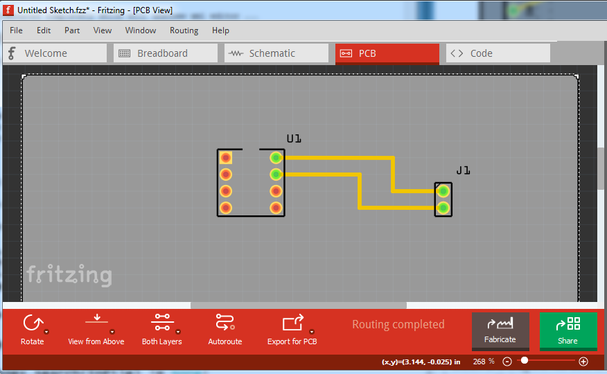
Welcome aboard! I’m actually surprised that auto routing did this well our usual advise is don’t use auto router as it usually does poorly. Being as it did work reasonably well in this case, you can either ignore the advise about 45 degree corners (it only typically matters at rf type frequencies) or edit the sketch and drag the red dots to make another bend point at 45 degrees like this:
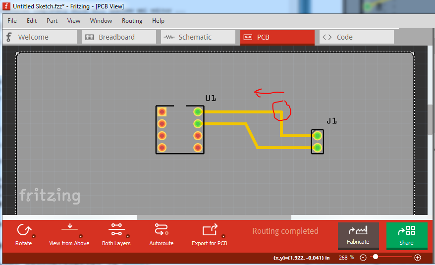
Click on the corner circled in red, then drag it in direction of the arrow til it is 45 degrees. I remember a key sequence that (cntr-shift?) that will snap to 45 degrees but that didn’t work for me in this case but a search in the forum search bar for something like “snap a pcb trace to 45 degrees” may turn up the correct advise.
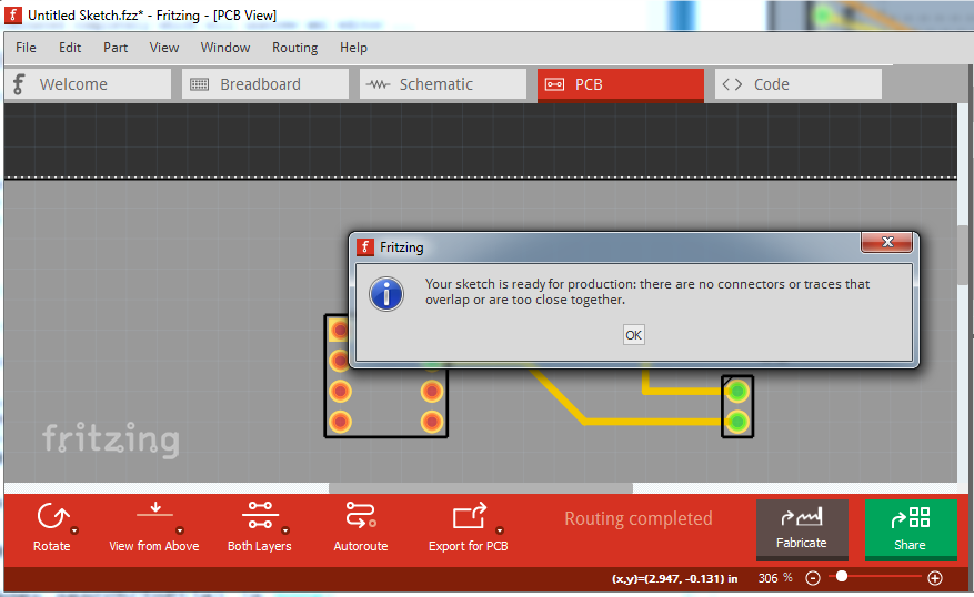
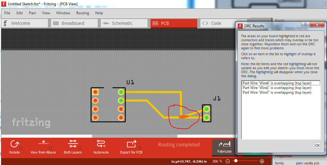
Where the red in the red circle indicates the overlap. Once DRC passes then you want to do File->Export for Production-> Extended Gerber, supply a directory (I usually use Gerber), and click OK. That writes the gerber files (which will be used to make you board) to the directory. You then want to examine them with a gerber viewer (I use gerbv from the geda project, but there are lots of others) to look at the traces as this (rather than the Fritzing pcb view) is what the board will look like. If you run in to problems post the .fzz file via the upload buttom (7th icon from the left in the reply menu) and one of us will have a look at it.
I do not know what other constraints your project might have, but the PCB traces simplify drastically (no autorouting), if you can either move the sensor connectors to the left of the ESP breakout, or swap the order of the connectors (so the sensors would connect the other way up). I filled in one layout for the schematic as well. I did not touch the breadboard view, but the same routing simplification as the pcb is possible.
A bit of part layout planning up front, or after you see where ratsnest line go, can make routing a lot easier. For you, or for autorouting. If your project has the flexibility, you can move parts around until the pattern of the ratsnest lines simplify before starting routing.
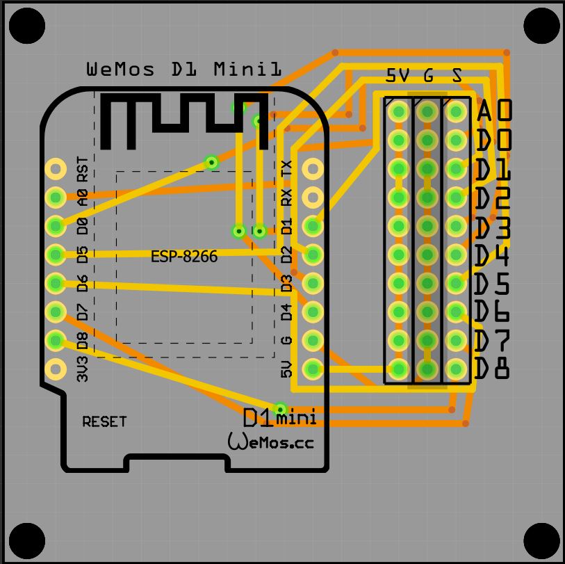
First item of business is that the Wemos part in core may not be the best. The holes in it are 0.036in where a standard .1 header (which is likely to be the interconnection) is 0.038in so the Wemos holes may be too small for anything except a wire. There look to be some alternate Wemos parts available on github or I could fix up the one in core parts as a new part. Then there doesn’t appear to be a power source in the sketch. It could be that you are intending to supply power via one of the servo connectors on the .1 header, but all of them have signal connections to the signal pin and normally the senor (or servo) wants power and ground to operate, so there should be a 2pin header that supplies the board with 5V (in the form of a 5V and ground pin) I expect. In this sketch I cleaned up the routing somewhat and added a two pin power connection, but didn’t do anything about the hole size in the part.
Thats is such a simple fix, and i hadn’t even considered it, its is purely as a breakout board for the di mini, so location has no impact at all.
thank you for both those suggestions.
Thank you for the feedback
for some reason I had assumed that the holes would be based upon DuPont sizes as those are what comes with the d1 mini, my actual plan was to put a row of female duponts on the PCB and then insert the d1 mini into those.
The power I was going to take from the d1 mini from a USB 5v supply, as these are running milliamps I have managed this in the past when just using breadboards. that then also takes care of smoothing etc. BUT i am still learning and if an external supple would be better i am happy to adapt.
It may work fine as is, I haven’t seen any complaints about hole sizes too small against this board, but here is an improved part that has proper size holes (and a few other fixes):
You can load this part in to your mine parts bin, then select the D1-mini in pcb and click on “delete minus”. That deletes the mini, but leaves the traces. You now move the new part from the mine parts bin to the same position as the original (in all three views), but the connections will all be red (indicating no connection) in the mini. If you click on the trace near the pin of the mini and drag it back a bit then back on to the pin, it should go green indicating the connection has re established. In practice I sometimes can’t get a reconnection and end up deleting the wire and doing it again. Another option (since you used autoroute) is to select Routing->Select all traces then hit the delete key which will delete all the traces, then rerun autoroute and it should route again.
 our usual advise is don’t use auto router as it usually does poorly. Being as it did work reasonably well in this case, you can either ignore the advise about 45 degree corners (it only typically matters at rf type frequencies) or edit the sketch and drag the red dots to make another bend point at 45 degrees like this: