There is atmega 328 in fritzing but no atmega 328p. Can anyone tell where it is?
Hindol
As far as I know the 328 and the 328P are identical in pin out, so one part serves for both.
Peter
Thanks peter i will do it tomorrow only.
Hindol
Well, they don’t look the same to me. E.g., in the schematic it shows a square shape. Kind of confusing.
First, many chips come in different packages. The one shown in the image is DIP (Dual Inline Package). There are others that are packaged as SMD (Surface Mount Device) which are internally identical. Those are usually square packages.
Second, the schematic view has no need to look anything like the physical parts. That is a logical / electrical / functional representation. The only thing that needs to match, are the connections. Even that can vary, when a part has multiple pins that are connected together internally. Like ground. The schematic only needs one ground pin, if the part is created correctly. Also the schematic normally groups pins together by function, even if they are spread around the physical pins. So address pins are a group, data are a group, input are a group, output is a group. Ground at the bottom, power at the top is a convention for schematics. Sometimes the schematic representation for part aligns with the layout of the pins on the physical part, but that is not needed, and should not be expected.
You probably don’t know, but you have to be very specific because this is engineering.
It seams the 328P comes in 2 packages, so no one knows which one. Always look up the datasheet so you can explain things better. 
Hello Old. Might be that I have a few years on you though😁 Also, I am an engineer 3 time over. Most of my experience has been in software development, mostly scientific. Although registered as an EE (and ME) I never practiced in electrical. My meager efforts in electronics is all post-retirement hobby stuff. So, I have to confess that what I was hoping for out of Fritzing is apparently more of a wiring diagram rather than what’s called a schematic among the pros here. Also, datasheets are baffling to me. Sorry to disappoint.
So, I’m on the verge of giving up on Fritzing and going back to pencil & grid paper.
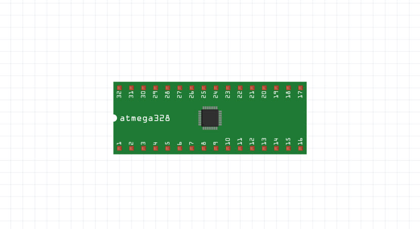
In what sense are “the 328 and the 328P identical in pin out,” when the 328P chips I have have 28 pins and the diagrams for the 328 in the Fritzing parts collection have 32 pins?
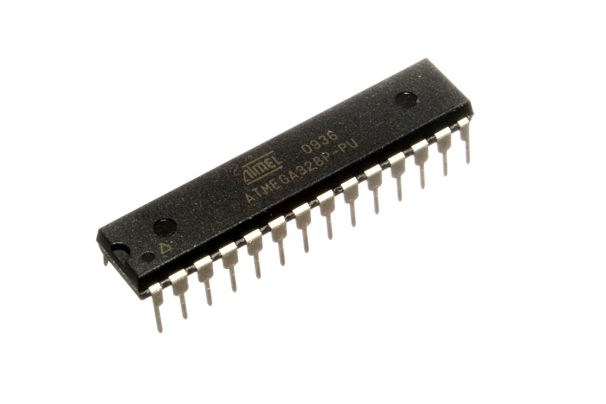
I have a bin full of these - all DIP form factors are the same. Specific ‘performance/electrical’ differences are identified in the Spec. Google “Atmel 328p spec” The spec covers all 328 types.
fyi in my stock parts bin
That’s not a DIP. The DIP’s are 28 pin. Of course, you can use whichever you want. Look at the spec to learn why one is 28 and other is 32 pins (THT and SMD)…
Now I’m getting the picture. Following your example, I selected Varient DIP 28 THT and I’m seeing my chip!
Thanks!
Maybe you can think of the schematic view as more of a functional block diagram, while the breadboard (and pcb) view are more of the implementation details. Same pieces, different perspective.
Data sheets can hold a lot of low level details. The trick is to filter, to get to the pieces that are currently of interest. It is all important depending on the context, but a lot can be ignored if you are not approaching the boundary conditions (min/max temperature, voltage, pin load current, timing limits, …). Most hobby projects are safely ‘middle of the road’, with wide margins. When that becomes not true, the datasheet will show where the walls (and cliffs) are going to be.
The image you show is a carrier board to allow an smd version of the part to be used on a breadboard. I did not check pins, but probably makes it a plug in replacement for the dip package.
Remember that the people that created the Fritzing parts have different needs and perspectives. I would not have bothered creating the breadboard view like that. If it is really a drop in replacement for a dip package. I would have used the standard dip package in the breadboard view, but with the SMD footprint for the pcb view. So prototyping on the breadboard could use the dip package, or smd on a carrier, and the final project pcb board could use the smd package.
Just my perspective. I can’t add “engineer” to my credentials, but I have a computer science / software programming background, plus working with electronics going back 50 years.
Thanks, Merlin. I admire you background. I try to make up for what I lack in knowledge and experience with determination and persistance 
A moving target. My background does not have some of the official education, but I learned how to (usually) find answers to new conditions. Google is your friend. Once you know enough to figure out what the right question is.
I started 5 years ago, and most of the numbers in datasheets are baffling to me also. The easiest part is the package, because it’s a pic. Like the 328P has a TQFP package with legs, and a 32 MLF with pads, and they usually have an engineering drawing at the bottom for the copper pad footprint to use for each.
I’m doing some tutorials on how to use the FZ advanced features right now, and have some part making ones at the top, if you’re interested.
I’ve bookmarked the tutorials.