I am newbie around here but yesterday, after looking for the Arduino MEGA shield v2.0 fritzing part, I didn’t find anything here neither on google. The closest thing was this SVG Shield v2.4 on dfrobot forum website.
So I came with the idea of making it by myself and share it for fritzing (since I liked it). Using some templates from fritzing along with some part of v2.4 svg, I finished the breadboard for the v2.0.
It is usually best to upload the .fzpz file (obtained by exporting the created part). That is really a zip file that contains all the svgs and the fzp file that defines the part. The upload button is the 7th icon from the left on the reply menu. To upload an svg file it is usually best to rename it to .fzpz and tell us it is really a svg as the forum sometimes has trouble rendering svg files (which is what it tries to do with them). Given the fzpz file I or someone else will point out problems and how to fix them. There is also a python part checking script available on github (although I need to do some updating of it when I get time) that will point out some issues that it can find.
I am struggling about multiple things after following your tips, reading the documentation and the “new parts” tutorial.
First, here are the multiple svg files along with the .fzp file after trying to set up all the pins (took a bit to accomplish) inside the .fzpz one: Arduino_MEGA_sensor_shield_v2.fzbz (143.0 KB)
I tested it as you told me on the other topic and it has not loading error
But then here comes the problem:
The breadboard has a lot of header pins (G = GND, V = Vcc, S = Signal) along with the grey squared ones. Does that mean I have to define like +100 pins in order to make all of them work? I tried sharing the GND pins but wasn’t successful.
Following the first problem, I have to add the same ammount of GND (a.e) on my schematic file? There isn’t a workaround for it?
The board size is slighty misplaced when placing over the arduino mega board. Any quick fix for this?
I used the guidelines for the 0.1 inch separation between connectors and used the same PCB from the arduino mega 2560 rev3.
The board size is critical in PCB view, which looks fine, so you can leave the BB if you like or you can scale the BB in the X direction only. The MEGA header pitch seams ok, so only the actual board element has to be scaled, but are the inner headers supposed to be on 100mil because the gaps aren’t 100mil.
Yep, you need a pin in each of the three views for every pin on the board. Once you have all the pins defined you can bus all the VCC and GND pins together either in the fzp file or via the parts editor but you first have to define all the pins. That may be easiest to do (assuming you can get it to work, I usually can’t) in parts editor as that will create all the needed xml in all three views and most importantly assign sequential pin numbers while you do it.
If you don’t want the interior pins to appear in schematic it is possible to surpress them there with some work, but I expect you are going to want to be able to connect sensors in schematic as well so you will need all the VCC and GND pins to be present in schematic as well. I don’t think there is a workaround (certainly without a code change and probably not even then) for this. It is possible to stack connectors on top of each other in schematic but it will usually then be messy when you hook up sensors and I prefer not to do that.
The pcb svg looks like the spacing is close to .1 in as it should be, so I assume the pins are misaligned in x or y against a real board? There don’t appear to be any transforms on the pcb svg (which is the usual problem with scaling problems) so there likely isn’t a quick fix per se, you would need to ungroup the copper layers (because otherwise Inkscape will use transforms) and move select a group of pads and move them in x and y to correct the alignment. I’d start by exporting a copy of the original board you used and make sure there its pcb and/or bb (unmodified) is correct, its possible the part you cloned from is incorrect. If as Old_Grey indicated the problem is in breadboard, there you have some transforms which ungrouping everything should remove although the spacing in Inkscape looks correct. Again this part is exported as a bin (.fzbz file) rather than a part (fzpz file) which is preferable. Welcome to parts creation hell .
Yeah, I noticed something like that while looking for the .svg files and .fzb of arduino mega 2560 rev3 part. They defined every pin used on the connectors tab and assigned the pin based on that. Looks like a ton of work for me
I read something similar while looking on the forum. So basically, I go to my .svg file, add multiple “gnd” pin as example, all stacked on ine place and then… Something related to making them visible using a xml property.
I used the arduino mega breadboard as base layout but since the shield doesn’t have the extra space due to the usb / power jack, I just picked “fit to the drawning limits” on AI. Probably I should let the white space since it has transparency. The pcb is the same from the arduino mega, the missaligned one is the breadboard.
I was a little incorrect to say this couldn’t be automated. I have thought about (but not done anything about) a python script like the parts checking script that would take parameters like 120 pins and create the fzp and svg files with the xml for the connectors all defined. You would then need to use the svg editor to move them to where you want them, but at least the tedious editing work would be done. The right way to do it is finish the parts editor but that is a much bigger task.
Usually you don’t need any special tags, multiple pins overlayed on top of each other just work. I just find them messy and prefer to have them spread out (especially on something like this board with rows of sensor plugs) so that all the pins for a single part are in the same place.
On Inkscape (as noted I don’t know Illustrator, perhaps someone here who uses it can comment), we use the resize page to content button to reduce the viewbox to the edges of the defined component. If you don’t do that sometimes the scale gets off or the connectors are not aligned properly to the grid (although I’m not sure why that is). I don’t know how to do the same in Illustrator but I expect someone here probably does. I can fix it up in Inkscape for you easily enough, but if as last time that doesn’t translate well to Illustrator it may not help much.
Yeah, it would be useless due to the compatibility between both software. I saw something related to that on the documentation so better stick with Illustrator and try if I can fix it on my own.
Also, speaking of the github docs, while reading the part file format section, I found this:
The most annoying quirk with Illustrator is that Illustrator defines a pixel (“px”) as 72dpi, whereas in the SVG standard, a “px” is 90dpi. So when you save images from Illustrator, if you want them to show up at the size you expect in Fritzing, save the image in units other than px (and note that if you leave out units entirely, it means “px”). Fritzing does try to correct for this problem, but your safest bet may be to open your Illustrator-based SVG in a text editor and hand-modify the width and height attributes by dividing each by 72 and putting “in” (meaning inches) as the units.
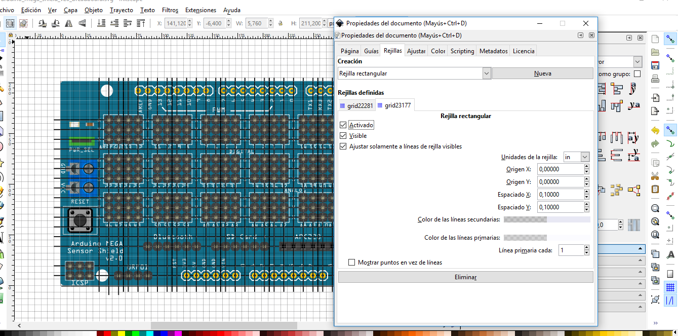
After looking at it, I set my file preferences on inch units and changed the dpi from 72 to 90 as stated above. So far, it has worked as my piece has the same size as the arduino mega breadboard. Does was that you meant when you do the “rescale” step previously mentioned on my other topic?
Then the schematic view should be huge than the current one. Not sure what to do, since there are like… 4x3x6 = 72 approximately GND pins plus another 72 for Vcc plus 72 related to the digital / analog. JIKES!
The right way to do it is finish the parts editor but that is a much bigger task.
I will not finish it right now, been handling some house-related stuff so I would focus on another simple part meanwhile. This weekend I will try it for sure
the dpi guess (which is sometimes wrong) only happens if the height/width of the view box is specified in px. If you set that to either inches or mm it doesn’t apply. The latest CSS standard has set the value to 96 from 90 just to add more confusion though. All of your files have had in as the units on the view box so that isn’t a problem. The scale is the ratio of view box to height/width so a 1in by 1in drawing wants the view box set to 0 0 1000 1000 so 1 px = 1thou. That is where scale comes in. I think the 96px / in is why the scale factor should be 10.41667 in Inkscape (rather than 10)
Yep they get a bit large. Have a look at the part in this post, it is similar in nature with 2mm grove connectors. I corrected the schematic to add the necessary ground, VCC and signal connectors. Its similar to what you need to do for this one. It had something like 136 unassigned connectors in schematic when I started …
I meant complete the code to implement the rest of the stuff that parts editor is supposed to do in the source repository rather than just using the parts editor …
I found a quick way to do it! While checking the arduino one breadboard, I noticed there is a option below the connector list called “Show internal connections”. Basically, you don’t have to set all pins but only the required ones 1 time and then check this option.
Green lines will be drawn after dragging one pin to another. No need to do the whole +300 unassigned connector list the same goes for pcb and schematic mode.
There is usually several ways to do something in fritzing so as long as it works use the method that works best for you. I’ve never had much luck (possibly because I didn’t spend enough time learning about it) with parts editor so I don’t use it a lot.
The struggle is real with this part editor since the “show internal connection” option just help you to interconnect several pin but you must manually assign them into the breadboard.
You may want to check Old_Grey’s tutorials I remember comments about parts editor being able to assign sequential pins (however that may only be to preexisting connections, I’m not sure), because I don’t tend to use it doesn’t mean it won’t work for you. @sublimeartistry uses the parts editor exclusively to make parts and is very happy with it. He may be able to suggest a way to do this in parts editor (it may be that you need to start with an initial part with sufficient pins though if I remember correctly, I don’t think parts editor will create new pins but I could well be wrong).
Yes it got much larger, but it worked for the poor person trying to do a project (I think for school) which the original didn’t. Not having wires cross and be messy is exactly why I did it that way. All the ground and VCC pins needed to be there either all on top of each other (which I don’t like) or separated as I did it so the work is about the same from my point of view and I think my result looks better on the schematic.
Sorry I didn’t read all of the post, but I think you can assign pins in XML. I think you duplicate the node and call it connector"#"pin or pad. How you relate the # to what pin I don’t know, but I noticed that some parts already have pin assignments.
I remember doing a simple svg drawing - no labeling nodes - and assigning pins in FZ Edit Part, and when I exported it had all those connector#pin automatically added. Maybe reverse engineer that.
It is true that I do use the editor exclusively but it is also true that I do not use Breadboard at all and I never do modules either. The only thing I make is parts for making PCBs. This means when I do it I usually start with a generic part or a mystery part and only change the PCB svg and assign its pins. So the BB svg and SCH svg already have all their pins assigned and I only have to assign the PCB pins.
There are a lot of messages on this thread and I’ve not had the time to read all of them; just to say:
I created the latest version of the SVG and had intended to turn it into a working part, but ran out of time. If you have any questions about it I would be happy to help. I put a lot of work.into getting the layout right.
However, be aware that the pin alignment on the svg of the DF board does not match Fritzings Mega 2560 for two reasons: 1 the two actual physical parts are slightly different dimensions - they fit but there is strain 2.The dimensions for the 2560 part in Fritzing are wrong. I checked against the orginal.CAD files and I have a (modtly) complete revised 2560 part but never got that completely finished either.
Also note: DF change theIr boards a lot. Your work could very easily be wasted.
Hi mate, nice to hear that, the arduino mega shield v2.4 you designed was pretty good indeed. I tried to use it for the v2.0 one since it has similarities regarding header layout but I switched to fritzing arduino mega in order to make it fit correctly.
I did the other board parts as aesthetical as possible since I need it for my own university project. I couldn’t find the original .CAD files but doesn’t matter as I keep the grid spacing between them (except for the mega header connector).
As final opinnion, I have no idea about df board since I bought this shield from local store.
Okay, has been some time since I did some work for this part but I spent half day doing a lot of fixes based on the original Arduino mega board file. Basically, updated the header positioning on breadboard and pcb view and added the connector ids using Atom Editor which helped me a lot due to features like Find and replace using RegEx (and selecting all results with Alt + Enter), Sequential number package and beautifiers. The same stuff was used for all internal connection in BB view.
So far, the only thing left is renaming the pin in connector section and the big schematic view which I don’t want to do since there are like 325 pins! OMG!
The bad thing about internal connection with so many pins is that Fritzing can lag a bit while doing it manually.
EDIT: I forgot to attach a screen I took while doing it.
Last update: Finished the schematic part and made little fixes to breadboard. I am not sure about how schematic pin / terminal thing works but it doesn’t assign to the end terminal the correct wire alignment.
It looks like your problem is the fzp file. The terminals look to be there and correct in the schematic svg, but aren’t in the fzp file. For example connector9 (the first one I happened to try in Fritzing ) looks correct in the svg but the fzp is missing the terminalId tag:
So your easiest solution is likely to use a text editor to add the missing temrinalId fields to the connectors that don’t have one in the fzp file. The part check script provides this somewhat (because it lacks a connectorId) warning message:
Warning 14: File
’part.arduino_mega_sensor_shield_v20_bd1049fc611e766457ee7b1378778293_10.fzp.bak’
At line 4910
terminalId missing in schematicView (likely an error)
for all the missing pins. You would need to edit the fzp file and look at line 4910 to discover that this refers to pin 323 (big part!). I’ll add this to my list of things I should fix in the script, since it knows the connector number and could (and should!) display it in the error message to be more helpful. I think @Old_Grey 's solution with n/s/e/w in parts editor will also add the terminalId field however I usually have difficulty making that work so am more inclined to edit the file. As always what ever is easiest for you and works is the right answer.


 ) looks correct in the svg but the fzp is missing the terminalId tag: