Someone on github requested a couple of Arduino parts. Here is the first one, a Arduino GIGA-R1 WIFI.
edit:
I have replaced the original part with one that has pcb view although because it was partly created from a jpeg image it may not be accurate. If someone that has a board would print out the pcb footprint, compare it to a real board and provide corrections that would be appreciated.
thanks a lot for this great part.
The PCB view currently uses the breadboard file, I guess that was intended, to get the most important use case covered?
For an integration in Fritzing I would replace this with a PCB footprint that could be used for a shield.
I considered that, but there isn’t enough information available to do so. Breadboard is built from a jpeg image and I think the pads are more or less correct, but they likely aren’t accurate enough to be useful as a pcb, so I chose to suppress pcb instead.
This looks mostly good. A couple of issues, there is a duplicate breadboard svg in the fzpz but they look to be identical so deleting one will fix that. How did you figure out where the pads should be? I couldn’t find any documents that showed that and it isn’t the same as a mega (which is what I expected?)
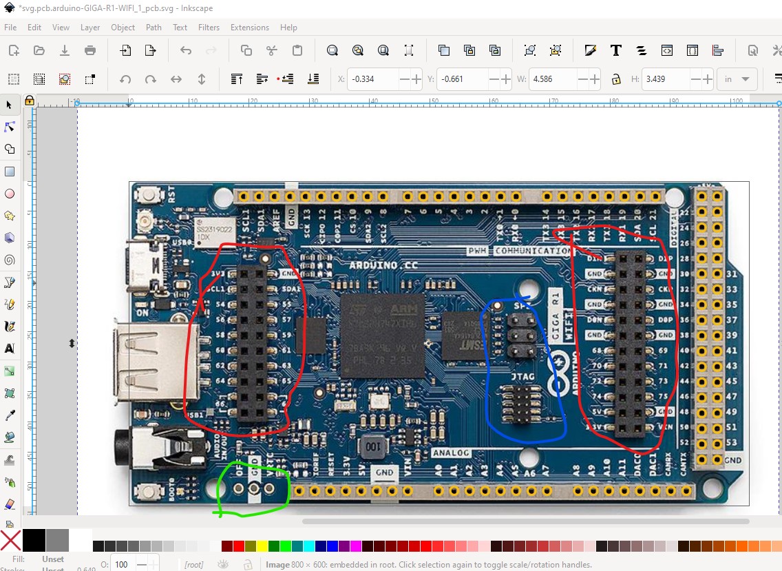
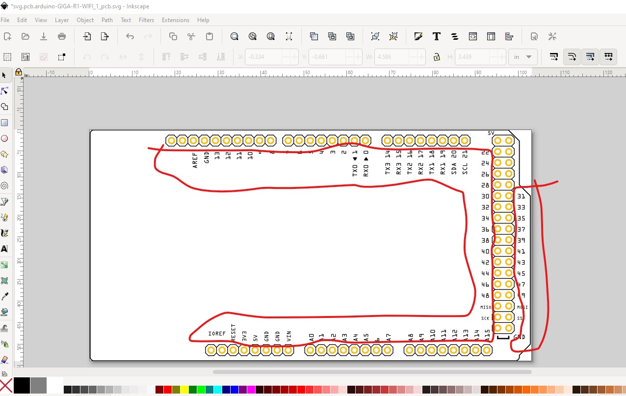
This is a jpeg image of the board overlaid on the pcb svg in Inkscape to check the connector alignment. I think we want to add the two connectors circled in red (assuming we can find accurate positions for them, and the bottom power connector (outlined in green.) It may be best to have pads at least for the SPI and Jtag connectors in case the shield won’t fit because the pins hit the bottom of the board. As well typically the text (and probably the outline lines around the connectors) are deleted because you can add them to the sketch if you want them, but you need to modify the part to delete them if you don’t want them for some reason. Other than that I’m in favor of adding the pcb svg to the part to make it better!
The part looks very good. My only concern is that the schematic view follows the pin order instead of being organised from a logic level. This is different from the current Arduino Uno R3 part in the core bin, which is organized by analog pins, DIO pins and power pins. I would prefer if the SCH view is organized logically as the schematics will look much cleaner and it will be easier to locate the pins (which is quite relevant in these kinds of parts with more than 100 pins).
The same applies to the Arduino Uno R4 minima and others. I think it is easier to fix them before adding them to the core than later.
Where as I prefer matching physical pin order so from the schematic I can identify the pins position on the physical board while troubleshooting without having to change to breadboard view (and find the associated pin) to tell where it physically is ( and I made this schematic so it is my way although that can change if we decide abstraction is better.) This is one part of the policy discussion on github which is currently going slowly. That discussion really needs to be completed before we have stable ground to base an update to core parts on. I expect we will find lots of other issues to resolve as well, as there are lots of things to consider.