I was wondering if anyone had any advice as to a potential workaround to create a 4-layer PCB in Fritzing?
I’ve made several 2-layer PCBs and I would now like to attempt to create a single board, featuring all these circuits and use 2 internal layers to form connections between the vias/headers as there isn’t enough available space on the outer layers.
Since you can’t explicitly create a 4-layer PCB in the software, is there a way in which I could create two sets of Gerber files (outer layers and inner layers) and then edit/combine them so that they would technically be a 4-layer PCB (as far as production is concerned)?
Any advice and information would be greatly appreciated - I really don’t want to have to draw up 10 circuits again in another package.
I’m guessing as long as I don’t have crazy vias that goes thru only few layers,
make all vias all thru, I can exported twice and assemble some 4-layer settings from the files
'cause I can maually do that with two 2sided board glued to gather and hand-solder some vias.
If I had extra layers for Vdd and Vss that’ll be much easier to make smaller boards
or maybe even with BGAs.
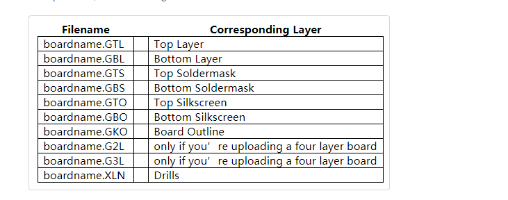
I don’t see any reason that shouldn’t work (with the warning that I don’t often do boards) as long as you know what to rename the two new gerber layers to. Tell us how you make out .


 but the info helps