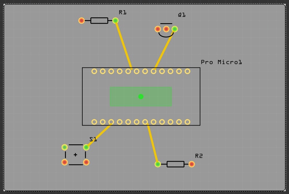
Ich möchte eine Leiterplatte für Arduino Pro Micro erstellen, jedoch bei den Verbindungen zu diesem verlaufen alle Leitungen auf der Leiterplatte in die Mitte des Microcontrollers.
Beim Schaltplan sowie beim Breadboard habe ich keine Probleme die I/Os anzuschließen.
Vielleicht kennt jemand das Problem und kann mir behilflich sein.
ich kann dir zwar leider nicht helfen, da ich Newbie bin, hätte aber auch gerne den Pro Micro in der Bauteilliste.
Wenn Du mit Deiner Bauteilerstellung erfolgreich bist, kannst Du es dann zur Verfügung stellen?
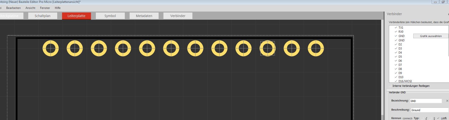
Most likely you have at least one unassigned pin… send me the files and I will look at them,
Update: I found a copy of the Pro Micro… It was pretty messed up, it crashed Fritzing when I imported it… I had to redraw part of it and reworked the files, but I think I got it. If there is any problems with it please let me know. Pro-Micro.fzpz (11.4 KB)
I only know the svg drawing program Inkscape, and in that you select Edit/XML editor.
In that certain nodes/objects have to be certain groups
PCB XML group structure.
silkscreen - non important lines/text that you want in the silkscreen
copper1
inside copper1 is copper0 - contacts and holes. Copper 1 is top copper layer on a 2 sided board and copper0 is bottom layer. Because Copper0 is inside Copper1 everything gets duplicated on top and bottom.
You are basically editing the XML file without having to know XML if you use the XML editor in Inkscape.
Make sure dimensions are correct in the PCB svg because it’s for production. It practically has to be a simple drawing engineering drawing.