Hi.
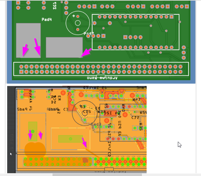
I like to add two large pads to solder wires supporting up to 50A current in the space marked.
What would be the best to create the connection (wires are too small) to the PSU connector and to the pads.
Regards,
Nils
Hi.
I like to add two large pads to solder wires supporting up to 50A current in the space marked.
What would be the best to create the connection (wires are too small) to the PSU connector and to the pads.
Regards,
Nils
The “pad” part, found in the CORE bin, in the “PCB View” section can be set to any size (width and height) using Inspector. The width of a copper trace can also be set in inspector up to 48 mil using the dropdown. It can be set larger than than by typing a value into the box, instead of selecting from the dropdown. One of the messages I saw said up to 128 mil, but I was able to set it to 999 mil. Very large sizes are likely to interfere with close by connectors. There is no control over the shape of the copper around the end of a wire. It is always a semi-circle. If you need more control, a custom part could be created, with a custom shape and connection point (connectorterminal) for the pad.
Having big solder pads is not going to help much by themselves. The current will still need to get through any traces and pins leaving the pads. Ground Fill can help some, but the rest of the (power) traces and components need to be able to handle the current too.
It is only a direct connection between PSU connector and PADs to solder wires onto. There is no component in between. I know now what you mean. I can see that the overlapping connections are looks not well in the PCB. Also the ground fill connection to the PAD is still very small.
Is it possible to draw a connection like shown on the screenshot in another tool? It seems fritzing is not the best for this.
Not sure if this is what you want but, perhaps this may help…
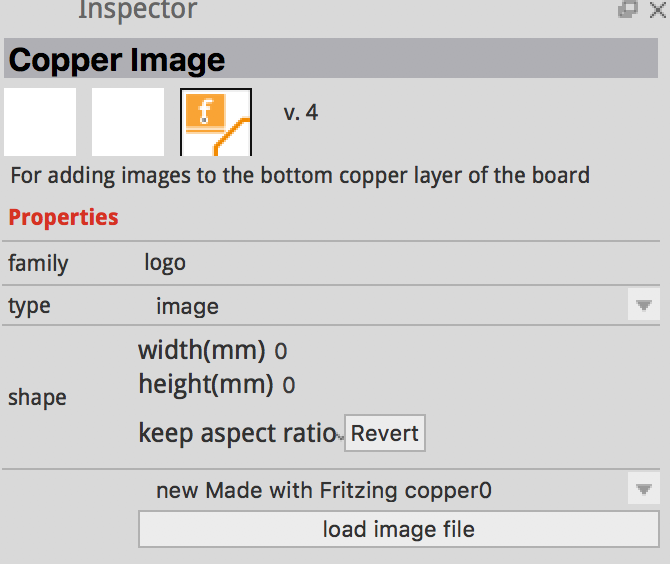
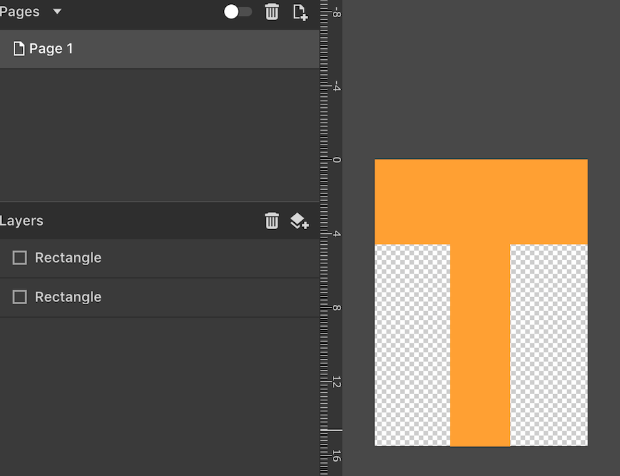
You can make a custom shaped Pad and load it into Fritzing using the “Copper Image” part.
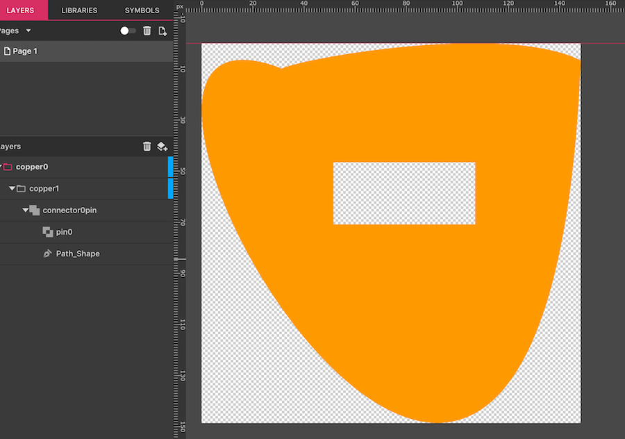
The custom shape must be SVG and best to use Layers as shown below. Can use most any Graphic/Drawing program.
The inner rectangle is a Contact Pin and can be any shape. Or, don’t have one if soldering wires to the pad… I show a Rectangle just a demo of ability to use odd shape contact…
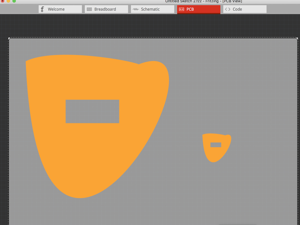
Below shows two: Original size and Re-Sized (by dragging corner handles).
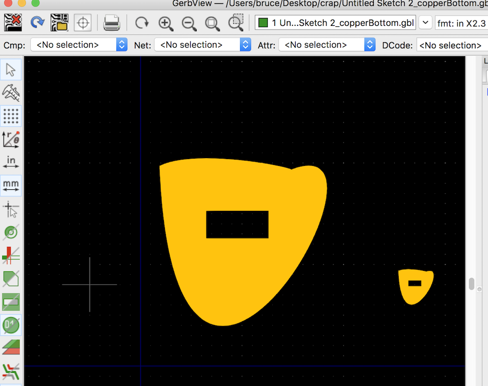
Also shown is result in a Gerber viewer (Bottom Copper Layer, thus, Flipped direction)…
Hi,
the pads itself are not the real problem. But I cannot connect it to the pins of the PSU in a good way. So at least I perhaps have to build a specific part with the connections designed to match the pins. But I cannot be the first one who like to build a higher current pcb like for RC Models… perhaps I will give target 3001 a change and check if it could be done there…
By the way I put a copper image on top the the pads but get warnings in the DRC and also do like have this copper visible.
More detail needed for what you mean by “in a good way”.
EDIT - see below…
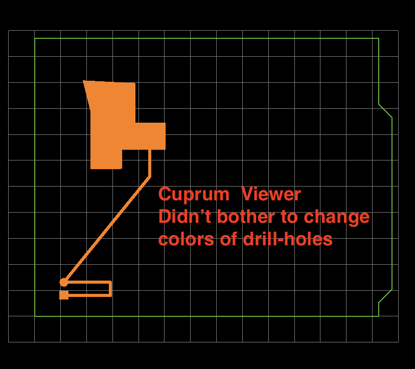
I’ll leave this topic with this: A Picture being worth 1000 words…
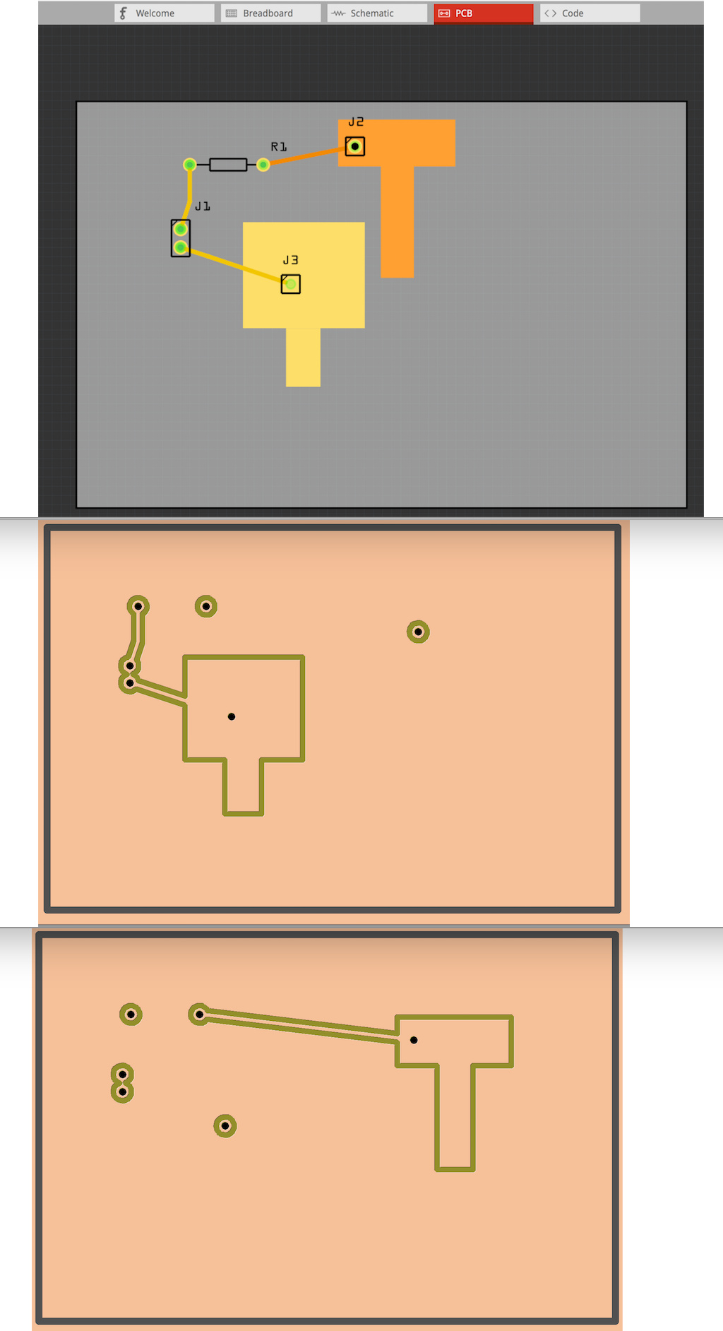
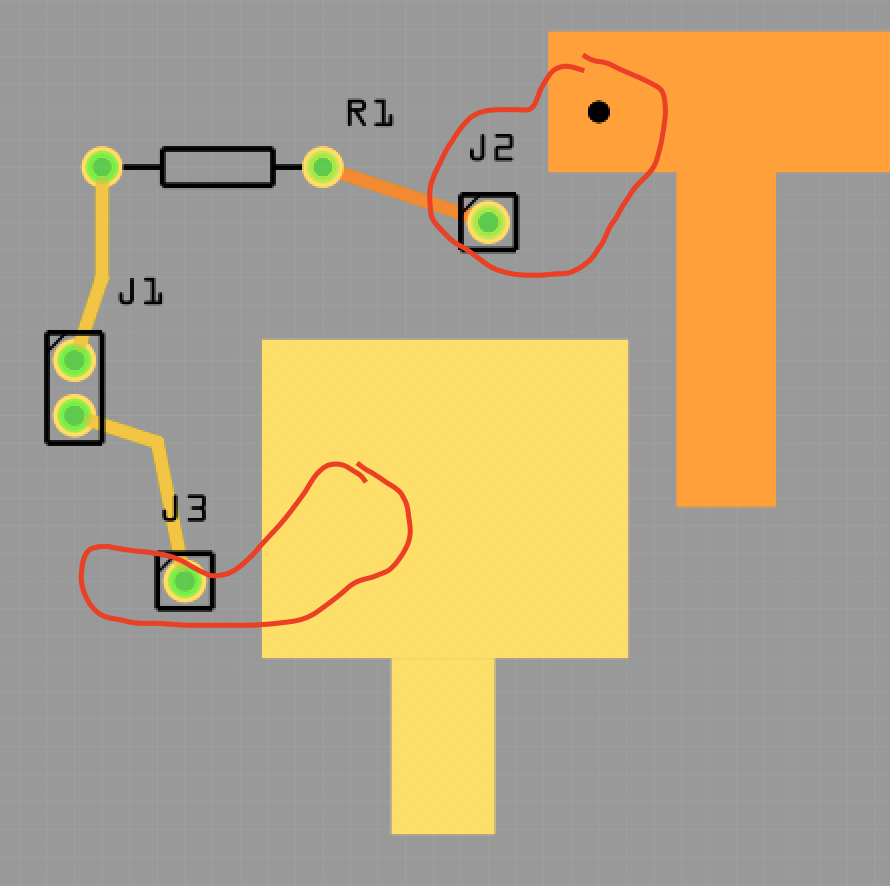
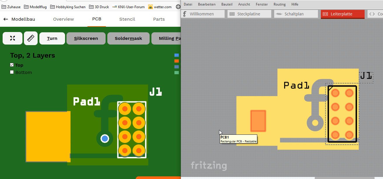
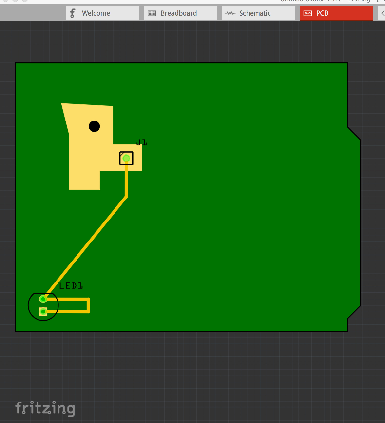
In Fritzing I added one Image to Top and Bottom copper layers;
I added a Pin/connector part to each.
I drew traces.
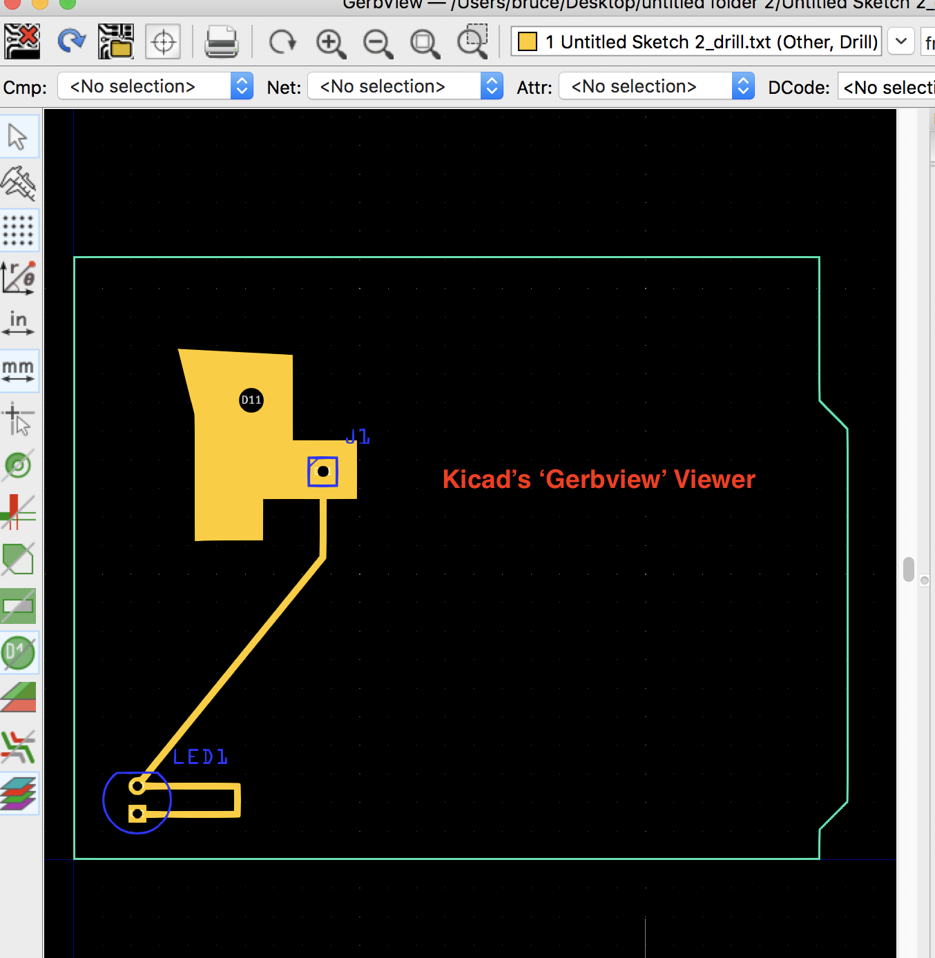
I exported Gerbers.
I loaded the Gerbers into the software I use to CNC mill my PCB’s
(I adjusted the offset to keep away from edges/contour)
Photo shows it all… Note: DRC is not very useful and will do what user sets in the pref’s. I Never use DRC. I always use my Eyes and CommonSense.
Thus, you can make most any kind of connection using whatever part you want…
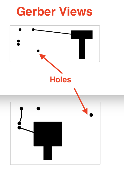
Note: you won’t see the contact holes cutting through the image you use - the holes show in the Gerber-layers and Drill files (example below) and in final usage (depends on the tool-chain software).
Top and Bottom copper layers shown below…
**EDIT Oops! been too long since I’ve used Frtizing and forgot: You can also add the “Hole” part over the Pin-Contact. That’s will make the hole show in the PCB image. I did that on the ‘T’ shape but, but Not on the larger shape. Last image shows them after moving the pins… The PCB fab will still have the holes if not using a Hole Part…
ADDITIONAL: You do not need to create the SVG with Layers. I did Not use layers for these the two graphics. Last image, below…
Hi know now how I can handle it but it is more or less a workaround. But most is as you described. I thought an uploaded image with copper visible but it is covered. So I can use the image to connect the pad with the connector. I have to ignore the DRC errors but in gerberer it looks fine. Also the pad is fully connected.  But would be nice to have this covered in the standard.
Regards,
Nils
I added info after your last post…
What SVG program could you recommend? I tried Inkscape but we did not made friends. Perhaps there is a very easy freeware?
Also do you know how to remove the solder mask of the picture component? I thinking of adding some solder to the high current connection.
PS. Found “LayoutEditor”. For small PCB its free and I can edit the gerber directly adding the copper and remove solder mask.
PSS. It does not save all layers as the layers are too large. Ahhh. Shit.
I use several Free graphic programs but, not all are equal to all tasks and it seems with every update, they develop new ‘bad playground habits’, with respect to Fritzing’s needs. Each requires spending time trying out stuff, solving situational problems and taking notes… I became a self-anointed SVG expert from it(LOL).
I stopped updating them and stick with what works for me (perhaps newer versions are good…)
I could list them but, without knowledge of Trick’s and solutions, you may become frustrated.
To be consistent with most Fritzing users, the SVG image below was done in Inkscape.
•File>New_From_Template>No_Layers
•TooL: Draw_With_Bizar_Curves_And_Straight_Lines
•Fill it with Gold color
•Select it, Edit>Resize_Page_To_Selection
•File>Save_As> (the drop-down: Inkscape SVG)
Loaded it into a “Copper Image” on Top Layer
Added LED, Hole, 1-Pin_Terminal
Made traces as shown
Exported Production Gerbers
Opened them in two different Gerber Viewers. Looks okay.
If having some company make the board, I recommend making a clearly stated Note about ‘No SolderMask’ over that section (use a sketch/drawing/screenshot with Markings).
I use BBedit to edit all my html/xml/svg/gerbers/…etc - no limitations for my needs. Thanks for the info.
The SVG, below you can right-click, save-as…
![]()