A6 Mini GPS/GPRS (GSM) Module.
Here Is the Part:
A6_Mini.fzpz (261.8 KB)
Your part has a few problems. It lacks (maybe because Inkscape can’t render the svg but it appears Fritzing can!) a breadboard layerId which will cause the part to not be exported as an image (svg, jpg etc.) The breadboard svg is dimensioned in px rather than in or mm and it looks like Fritzing is guessing the scale incorrectly as the pins don’t align to .1in boundaries. Since I can’t render the breadboard svg I can’t try and correct it.
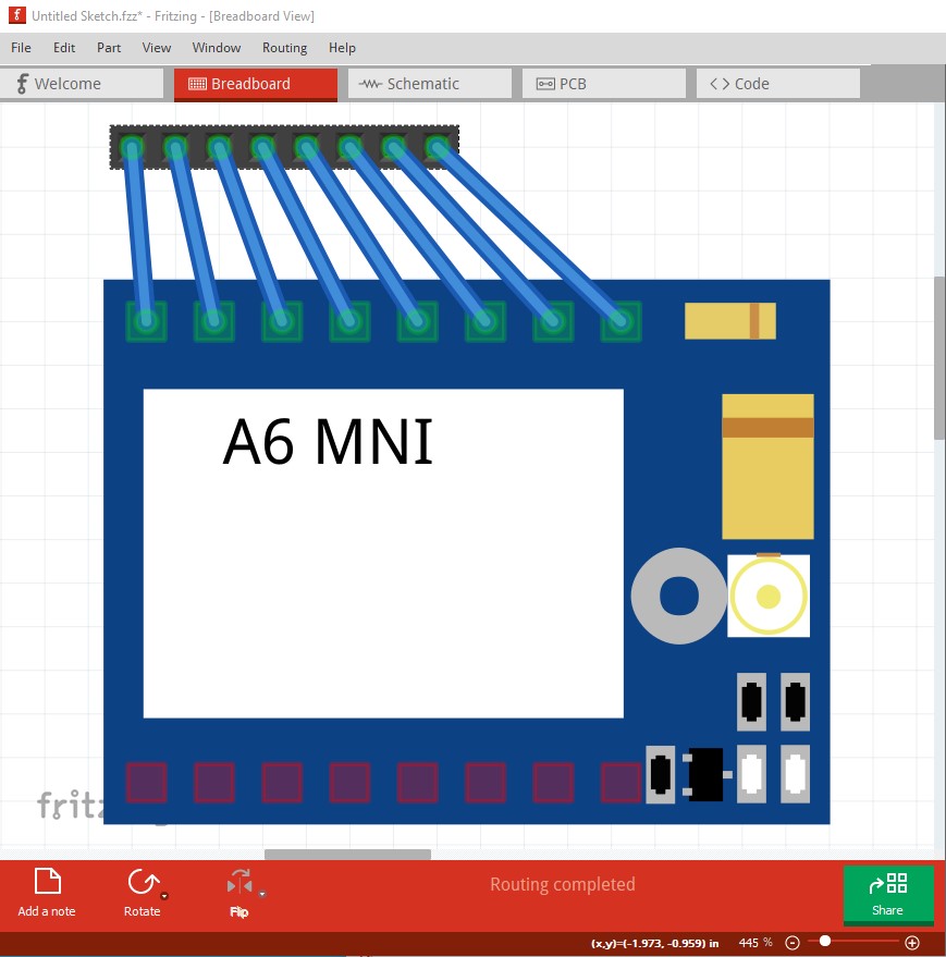
The pins should match the .1in header connector that is connected to it and (at least very probably) be on a .1in boundary in Y which it is not. In schematic view the terminalIds are defined as groups and thus Fritzing doesn’t recognize them and the wire then connects to the center of the pin like this:
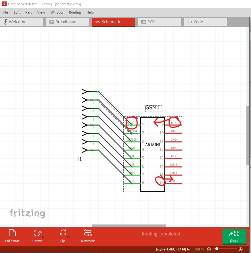
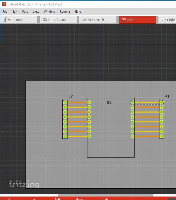
rather than the end of the line where the terminalId should be (typically a 10thou by 10thou rectangle.) In addition the pin number is typically on the pin in a smaller font and the pin name is on the inside of the box in a larger font. PCB should show the actual size of the board with the connectors in the correct place (basically a copy of the corrected breadboard) rather than the current IC outline.
Peter
So I should solve the size problem ( I should resize SVG into mm or inch).
Then I should solve the Schematic problem.
But I didn’t get your second paragraph
Since the data sheet indicates the headers are of .1in pitch likely breadboard should be as well. To fix the layerId problem the entire svg should be in a group with the id breadboard.
In schematic the terminalIds need to be a drawing element (not a group as they are now) for Fritzing to recognize them. The typical case is a rectangle 10 thou by 10 thou centered on the end of the pin where you want the wire to connect.
edit:
In the end I had to redo the entire part in Inkscape as whatever svg editor you used for breadboard isn’t compatible with Fritzing. Fritzing will parse defs correctly but I expect (but don’t know for sure) they aren’t part of the tiny 1.2 svg and your breadboard (even with the layerId added) won’t export as an image as the defs get deleted and the image doesn’t render. In this part (which has a new moduleId so will load beside your original) I started from a jpg image of the board and placed the pads in the apparently correct place (it needs to be checked against a real board for accuracy though!) I used Randy’s Inkscape schematic extension to make the schematic (because it formats the schematic correctly with little work) and copied the breadboard layout in to pcb (and modified it to be a pcb layout) so pcb matches both breadboard and the real board. The end result looks like this:
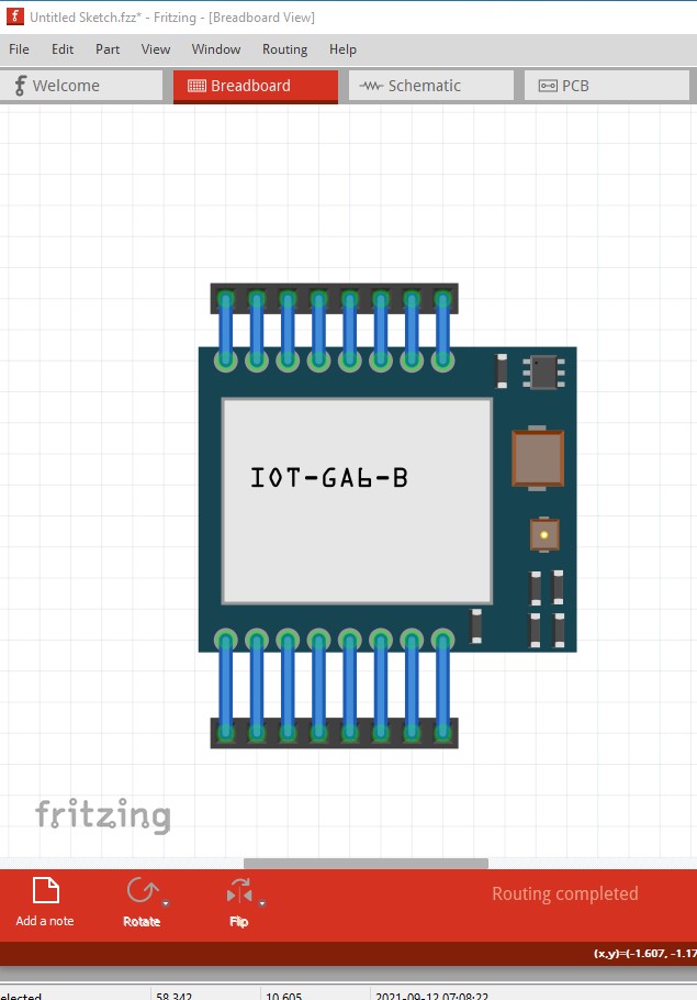
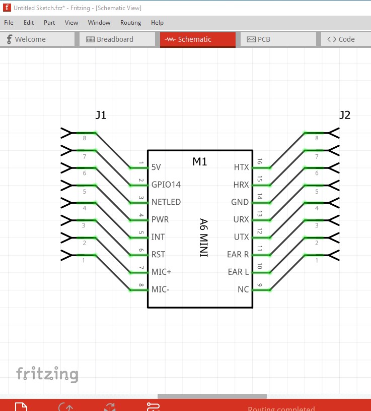
which came from this part:
A6_Mini-new.fzpz (7.7 KB)
If you unzip the .fzpz file you will get the 3 svgs and the fzp file that make up the part.
Peter