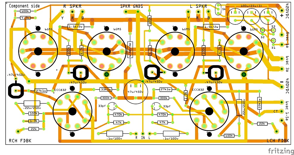
When designing a PCB for use with vacuum tubes, I always put the wires which connect the vacuum tube filament pins outside the PCB layout.
Does anybody have gained experience when including those tracks on the PCB layout?
I’m not sure I understand the question. Do you mean you connect the wires for the filament connection directly to the tube socket pin rather than run the traces on the pcb? I’d think (but I haven’t ever made a pcb with tubes) that a molex connector on the edge of the board to connect to the filament transformer (assuming you don’t want to mount the transformer on the pcb of course!) and reasonably wide traces to the filament pins (because I expect there is a fair amount of current in the filament circuit) should do. You likely need to keep those traces away from both the plate supply (for high voltage reasons) and the grid (for induced noise reasons) but other than that it should be straight forward. Hopefully someone who works with tubes will comment with a better answer!
Peter
Thanks Peter for your response and yes, you did understand my question correctly.
Yes, I do mean instead of connecting those wires directly to the tube socket pins, as I normally do, I want to apply a connector at the edge of the PCB and from there use traces to those tube socket pins. Those pins must indeed have width enough to carry about 400- 800mA AC current. The problem is that those wires also carry a stray field and normally, when using wires, I tightly twist them to reduce that stray field before connecting to the pins.
I was hoping that one or more of the forum members have gained experience how to do this when using traces on the PCB instead.
I was about to suggest ground planes and ground guard bands like this (crudely  ) as is done on the sensitive inputs to op amps:

where the bottom connector is ground and the top two connectors the filament (which may not be on adjacent pins!) Then I did a google search on “tube filament layout on pcb” and came across this article which has a bunch of suggestions I expect neither of us have thought of yet by folks that have done this:
https://www.eevblog.com/forum/beginners/designing-a-pcb-for-a-tube-amp/
The best bet seems to be your original tactic: external twisted pair wires, but note the comments on heat destroying the boards as well, that is one I hadn’t thought of. Using DC for the filaments is another good suggestion (removes the AC current that causes AC induction noise from the board.) It looks like 2oz copper and thicker FR4 would both be a good bet as well as leaving a bit of space under components like resistors to try and reduce heat transfer in to the FR4. There are a bunch of other articles on the subject in that search and some of them may have more info. I expect some of those forums are likely to have better answers than Fritzing as well, as I expect we don’t have a lot of tube folks here, although there are some. Good luck!
Peter
Thanks Peter for your valuable response. I certainly will study that link you supplied to gain knowledge on filament layouts on PCB’s.
Joe.
A late thought on the DC filament supply would be to use one of the 2A buck switcher modules to provide regulated DC for the filaments. That would allow putting a bridge rectifier and large electrolytic cap after the filament transformer (which will produce about 9V DC) and then using the regulator to lower the DC voltage to 6.3V (which should be equivalent to 6.3V RMS AC) for the filaments but without the AC current variation which should eliminate the 60HZ induction.
Peter
“…one of the 2A buck switcher modules to provide regulated DC for the filaments.”
Do not know what kind of circuit you have in mind here. But what I do NOT want is a switch mode power supply due to stray of disturbing signals those switching regulators produce.
Something like this:
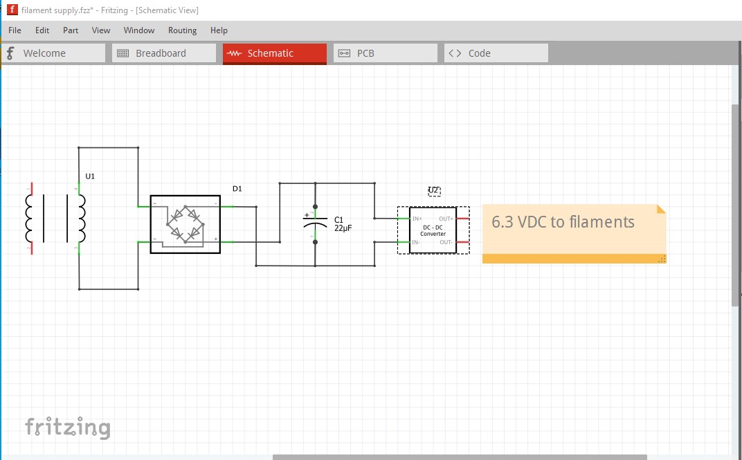
although the cap needs to be something like 10,000uf to keep the ripple down (which Fritzing wouldn’t let me set.)
filament supply.fzz (29.9 KB)
While it is true switchers create HF noise, it is a matter of where the noise is. In this case the switcher can be near the transformers which are already creating noise and magnetic fields but (hopefully) far away from the tubes, but the DC output to the filaments (where the low level HF noise can be suppressed by ceramic capacitors) should keep the high power noise of an AC filament feed out of the sensitive circuitry. Almost an amp of AC current right beside the sensitive and high impedance grid circuit is likely to be a lot worse than a few mv of high speed noise (and magnetic fields as well) a long distance from the grid circuitry though I expect. Induction drops off with the square of the physical distance so a noise source physically far away is better than one close. This is of course theory, as I haven’t actually done this with tubes.
Peter
Joe,
Been a while since I’ve scrolled thru here, but the fritzing outreach email program reminded me that I owe a debt of gratitude for this free software.
To your point, if it’s of any value this late- I used trace width calculator below:
https://www.digikey.com/en/resources/conversion-calculators/conversion-calculator-pcb-trace-width
Grateful to Peter for help mapping tube sockets for fritzing last year- I’ve made 4 diff design PCB’s w/ fritzing for my push/pull tube amp… they’ve all worked great.
Jim
ps. did Kjell ever figure out the att.net password email reset snafu?