Hi
Please find attached an IF transformer (42IF101) for parts submission and comments.
42IF101 IF TX.fzpz (5.8 KB)
https://au.mouser.com/datasheet/2/449/XC-600131-1212443.pdf
Cheers
KingKappa
Hi
Please find attached an IF transformer (42IF101) for parts submission and comments.
42IF101 IF TX.fzpz (5.8 KB)
https://au.mouser.com/datasheet/2/449/XC-600131-1212443.pdf
Cheers
KingKappa
There are a number of problems here. The most serious is that the pcb svg is not the correct size so the footprint won’t work. Here is a corrected svg

In the original the holes for the mounting pads are missing, the pin spacing is much to small and the hole sizes are also too small (0.016743in rather than the needed 0.030in) and as noted the holes for the mounting tabs are not present. I also changed the pads to pin (because this is a through hole part) and set the pin numbers from 0 to 4 rather than 0 to 5 so the .fzp file will need to change to accommodate those changes. The pin holes are 0.03in (the pins are listed in the data sheet as 0.027in) and the mounting holes are 0.06in. In addition the breadboard pin spacing appears to be wrong and it lacks a layerId, in schematic several of the terminalIds are missing resulting in the wires connecting in the middle of the pin rather than the end as they should be.
Note pin 4 appears correct all the rest lack the terminalId and thus connect in the middle of the pin.
Peter
Thanks Peter
The part with your corrected svg for the pcb.
42IF101 IF TX improved.fzpz (5.8 KB)
Cheers
KingKappa
Hi
Some changes from mm to inchs in the breadboard svg and terminal issues in the schematic svg.
42IF101 IF TX improved v2.fzpz (6.3 KB)
Cheers
KingKappa
A number of problems. FritzingCheckPart finds a number of errors as does visual inspection.
Warning 14: File
‘part.KK0000_e983535c73d542d6f35a90388924fc46_9.fzp.bak’
At line 127
terminalId missing in schematicView (likely an error)
Warning 35: File
‘part.KK0000_e983535c73d542d6f35a90388924fc46_9.fzp.bak’
Connector4 doesn’t exist when it must to stay in sequence
Warning 32: File
‘svg.breadboard.KK0000_c11fd98c36d97f05c059f4bb4dc4ec61_1_breadboard.svg.bak’
At line 3
Scale is not the desirable 1/1000 ratio from width/height to
viewBox width/height.
Warning 32: File
‘svg.schematic.KK0000_c11fd98c36d97f05c059f4bb4dc4ec61_1_schematic.svg.bak’
At line 3
Scale is not the desirable 1/1000 ratio from width/height to
viewBox width/height.
Error 69: File
‘svg.breadboard.KK0000_c11fd98c36d97f05c059f4bb4dc4ec61_1_breadboard.svg.bak’
At line 9
Found a drawing element before a layerId (or no layerId)
Error 69: File
‘svg.schematic.KK0000_c11fd98c36d97f05c059f4bb4dc4ec61_1_schematic.svg.bak’
At line 20
Found a drawing element before a layerId (or no layerId)
Error 18: File
‘part.KK0000_e983535c73d542d6f35a90388924fc46_9.fzp.bak’
Connector connector0terminal is in the fzp file but not the svg file. (typo?)
svg svg.schematic.KK0000_c11fd98c36d97f05c059f4bb4dc4ec61_1_schematic.svg.bak
Error 18: File
‘part.KK0000_e983535c73d542d6f35a90388924fc46_9.fzp.bak’
Connector connector1terminal is in the fzp file but not the svg file. (typo?)
svg svg.schematic.KK0000_c11fd98c36d97f05c059f4bb4dc4ec61_1_schematic.svg.bak
Error 18: File
‘part.KK0000_e983535c73d542d6f35a90388924fc46_9.fzp.bak’
Connector connector2terminal is in the fzp file but not the svg file. (typo?)
svg svg.schematic.KK0000_c11fd98c36d97f05c059f4bb4dc4ec61_1_schematic.svg.bak
Error 18: File
‘part.KK0000_e983535c73d542d6f35a90388924fc46_9.fzp.bak’
Connector connector3terminal is in the fzp file but not the svg file. (typo?)
svg svg.schematic.KK0000_c11fd98c36d97f05c059f4bb4dc4ec61_1_schematic.svg.bak
Error 74: File
‘svg.pcb.KK0000_c11fd98c36d97f05c059f4bb4dc4ec61_1_pcb.svg.bak’
At line 18
Connector connector0terminal has no radius no hole will be generated
Error 18: File
‘part.KK0000_e983535c73d542d6f35a90388924fc46_9.fzp.bak’
Connector connector3terminal is in the fzp file but not the svg file. (typo?)
svg svg.pcb.KK0000_c11fd98c36d97f05c059f4bb4dc4ec61_1_pcb.svg.bak
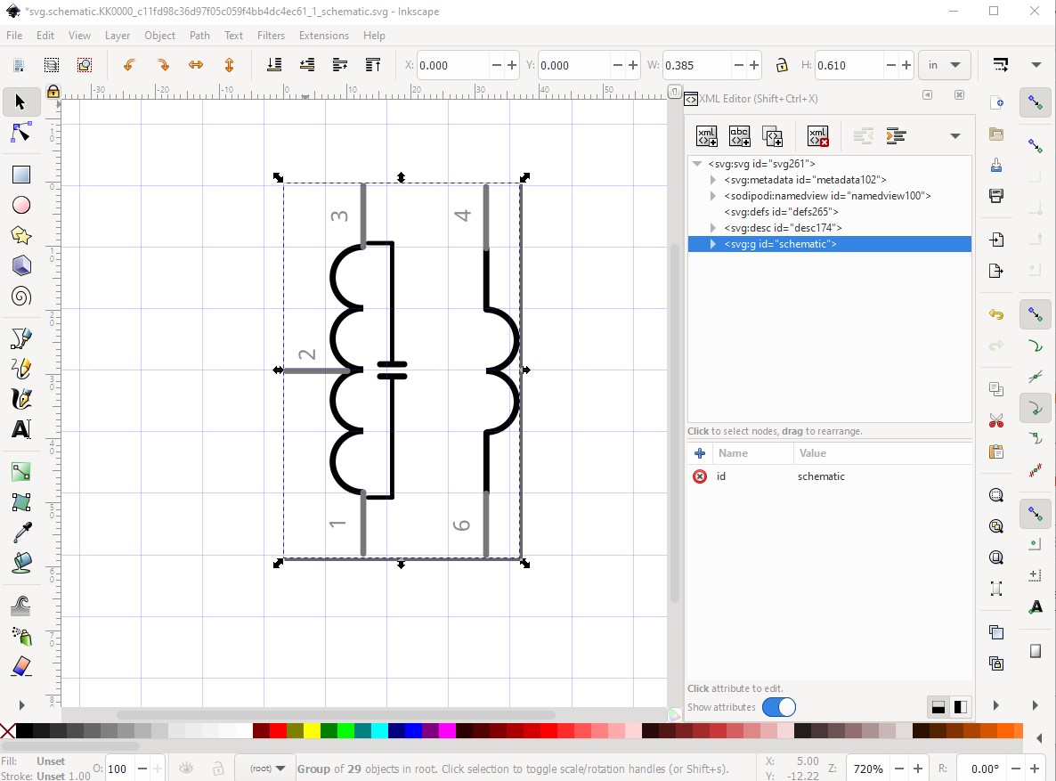
In this case the lack of terminalId in schematic is non standard rather than an error, but standard practice is to have the pin be 0.1in long with a terminalId on the end of the pin to indicate where the wire will connect. The missing layerIds will cause the part to not export as an image. In Schematic the pins are not aligned on a 0.1in boundary and thus the pins don’t fit the grid.
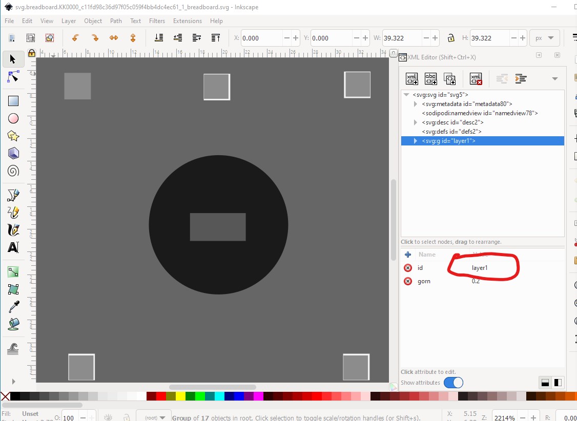
the pins with the red arrow need to move right by 0.05in to be on the grid. The pin (circled in red) is typically set as connectorxpin with a rectangle where the current pin terminates set as connectorxterminal to terminate the wire. The terminalIds missing in schematic will be ignored but they are not normally used in schematic. The connector0pin circle has turned in to an ellipse and thus won’t create a hole in the gerber output (making the pcb useless!) In breadboard changing the layer1 id to breadboard will set the correct layerId
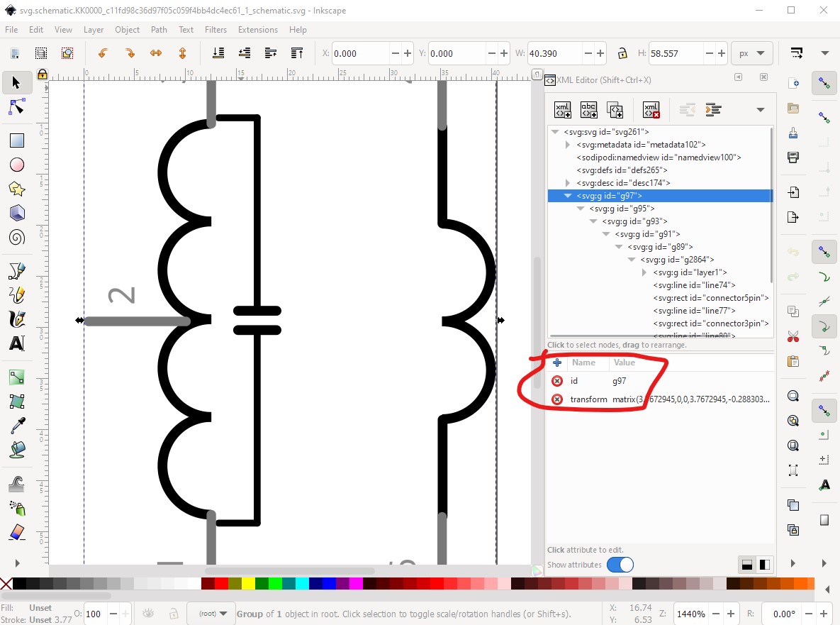
in schematic setting g97 to schematic will set the correct layerId, but I chose to ungroup to do the necessary other changes.
First rename the line to be connector0pin, then change the rectangle to be connector0terminal (you will also have to add a terminalId to the fzp file either by editing the .fzp file or using parts editor to set the terminalId) it should end up looking like this:
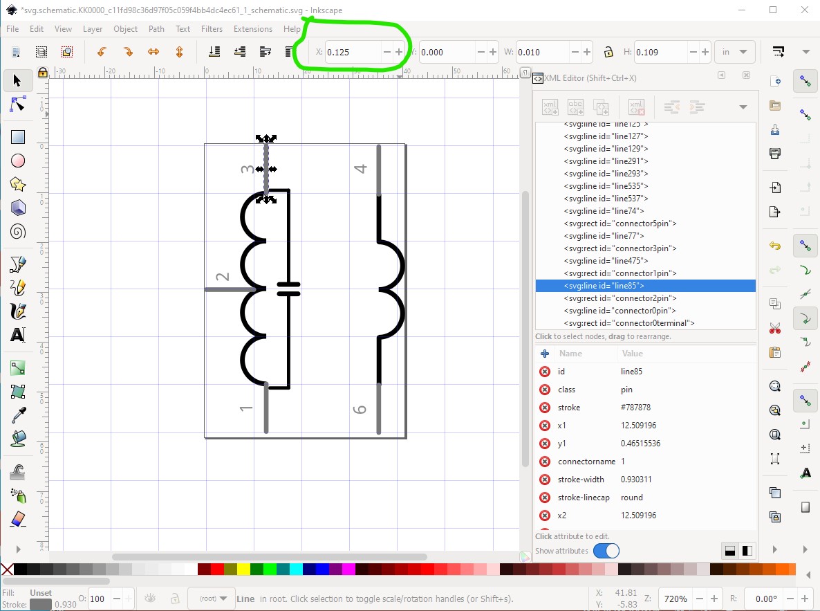
for all pins (here I just did connector0.) as well connector5 should be connector4 to keep the numbers in sequence. Then you need to shift the left side 0.05in to the right to align the pins to the 0.1in grid:
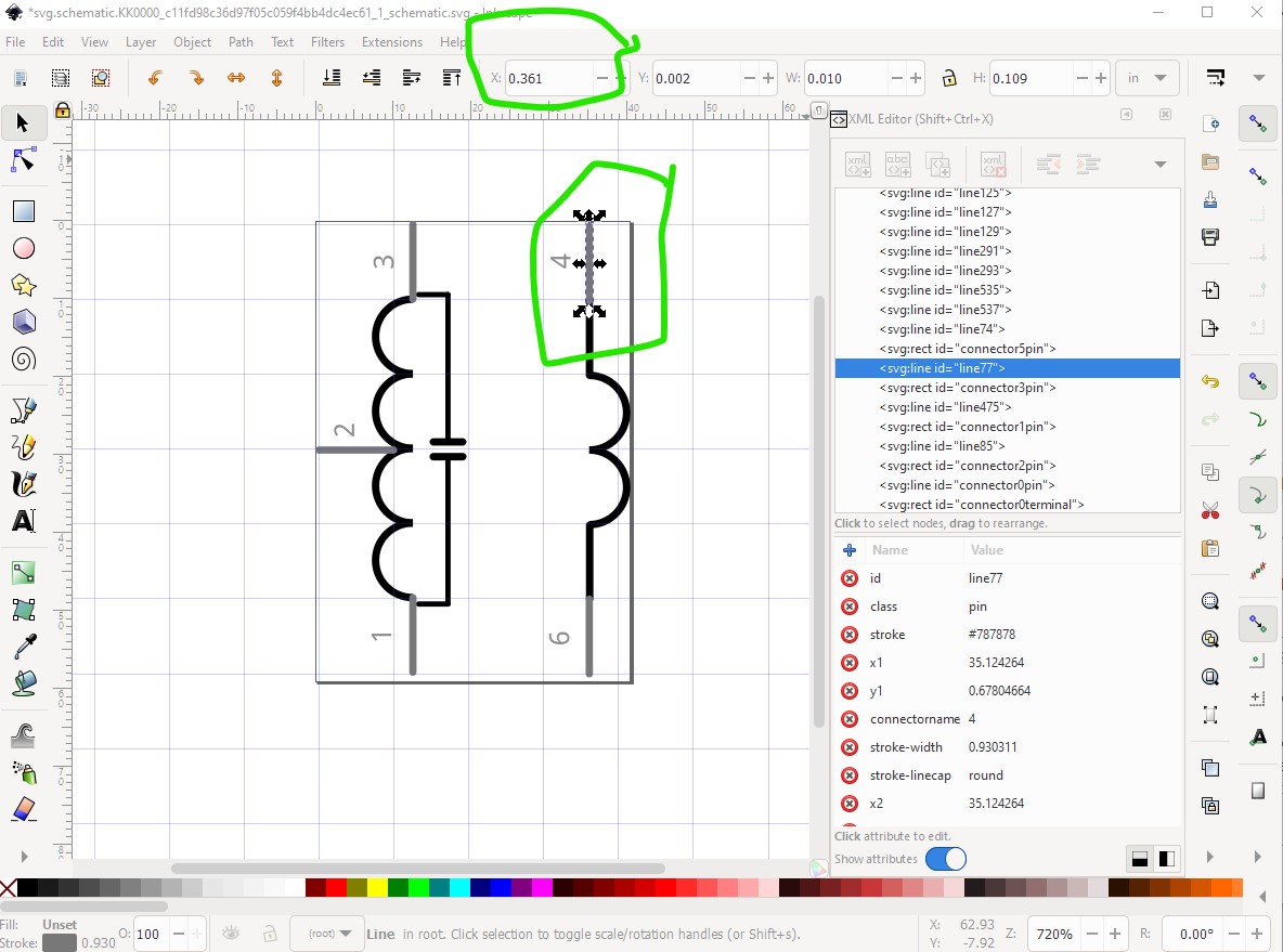
here the pin is at 0.125in in x, but the next pin is at 0.361in. To align the left side image needs to have 0.036in added to its x coord to bring it in to alignment on the 0.1in grid.
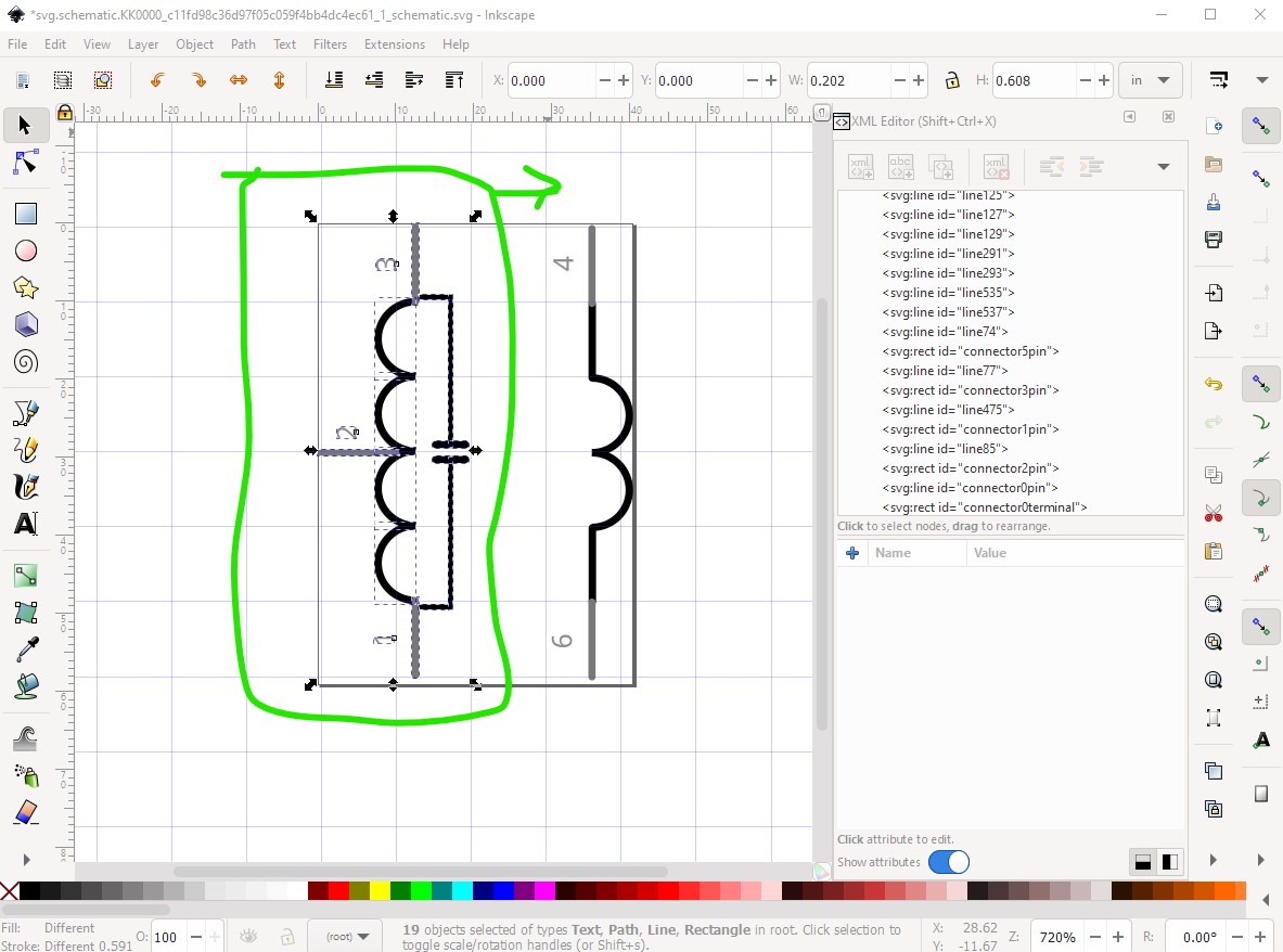
select the entire left side like this
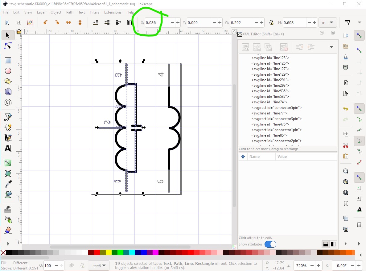
then add 0.036in to get this
which changes the pin 3 x coord to 0.161in to be exactly 0.2in from pin4 (at 0.361in)
Now do Edit->select all and Edit Resize page to selection to reset the viewbox, then Object->group and set the resulting group id to schematic to set the layerId and schematic is done.
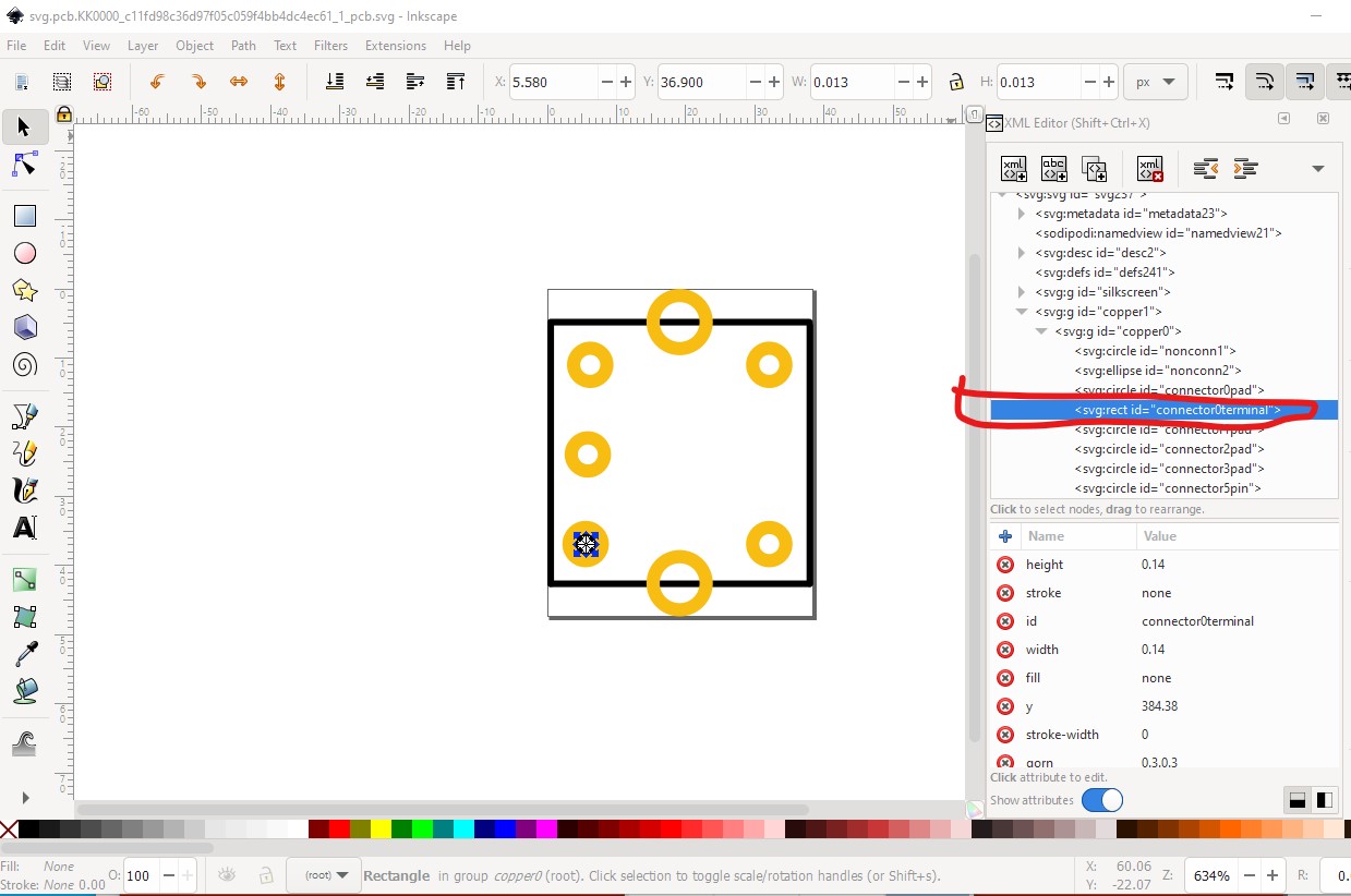
In pcb connector0terminal is not needed and can just be deleted.
in the fzp file the terminalId on copper0 can be deleted as it is unneeded.
    <pcbView>
      <p terminalId="connector0terminal" layer="copper0" svgId="connector0pad"/>
      <p layer="copper1" svgId="connector0pad"/>
    </pcbView>
should become
    <pcbView>
      <p layer="copper0" svgId="connector0pad"/>
      <p layer="copper1" svgId="connector0pad"/>
    </pcbView>
and that should do it.
Peter
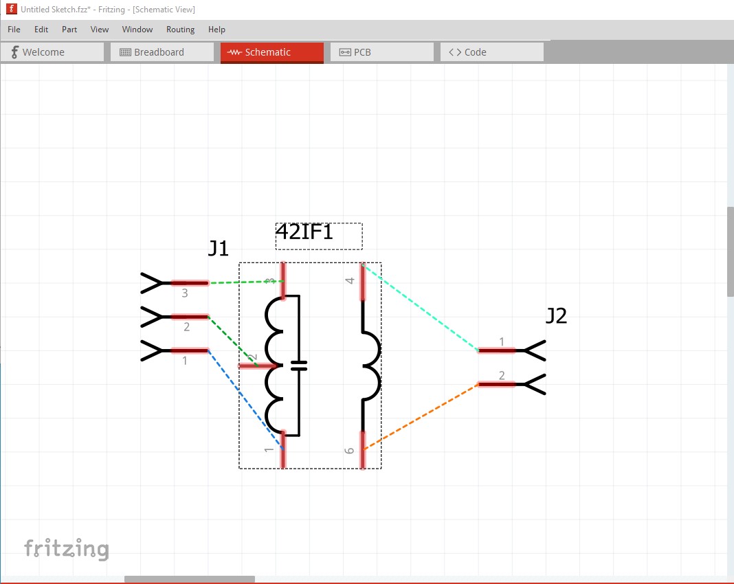
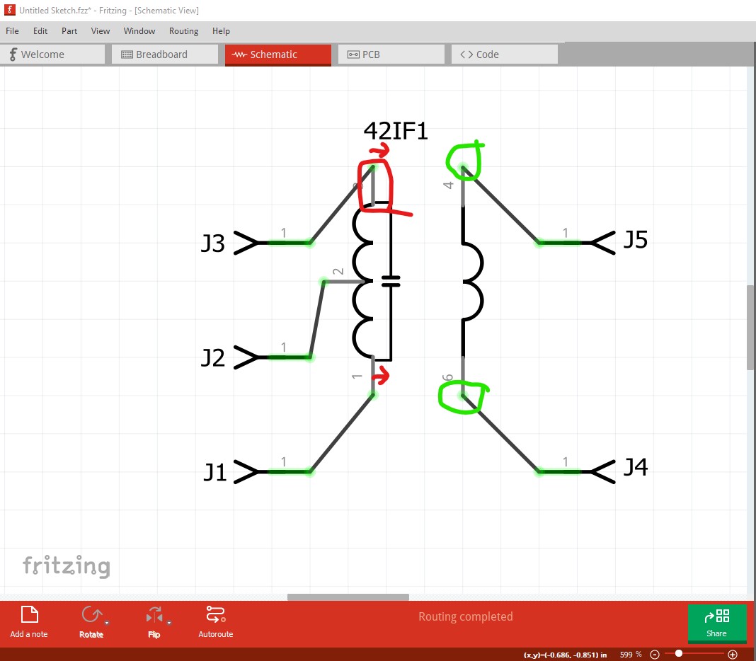
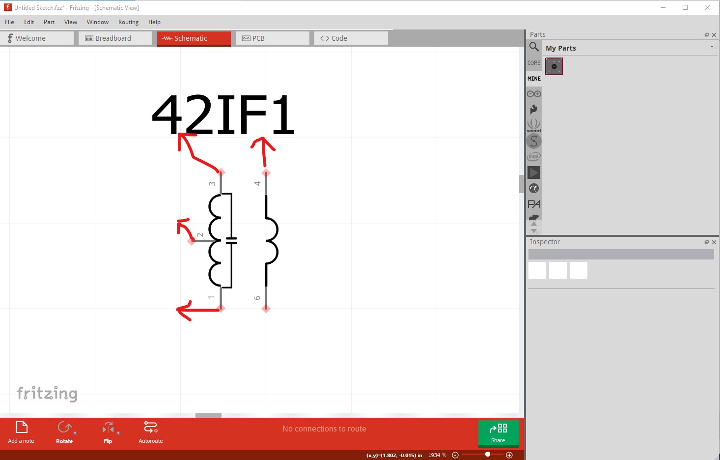
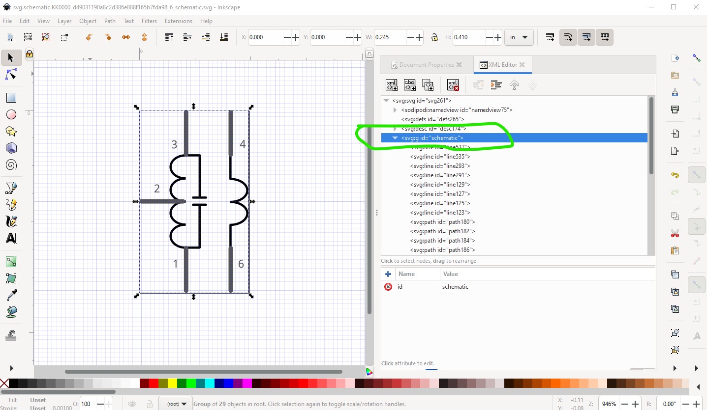
Still problems in schematic. It doesn’t align on the 0.1in grid and doesn’t have pins and terminalIds. As well the various colors don’t meet the graphics standards. This image from the part in Fritzing indicates the issues. The red arrows are where the various lines need to move to.
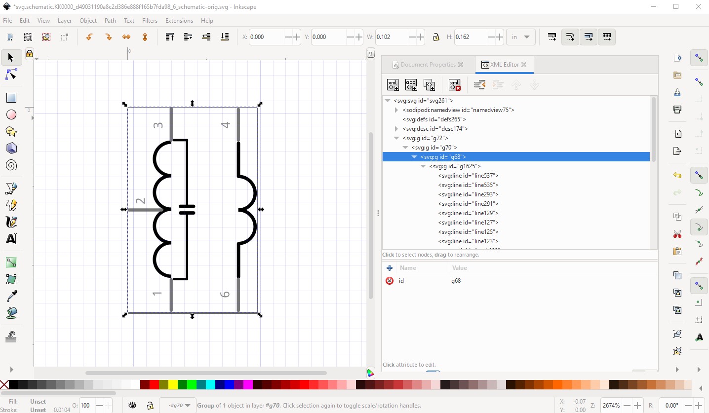
This is the original svg displayed in Inkscape. The grid is on 0.01in increments with major lines every 0.1in. The pins should align to the darker blue 0.1in grid lines and do not.
The group name outlined in blue should change to schematic to set the approriate layerId.
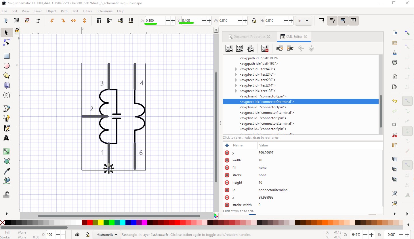
I loaded the svg in to Inkscape, then ungrouped it to make the following changes.
Grouped the finished svg and set the group id to schematic to set the correct layerId. Before that I changed the scale of the svg so 1 drawing unit = 1thousandth of an inch. Then I changed the name of connector0pin to be connector0terminal, and set its size to be 0.01in by 0.01in in the tool bar to create the terminal. Its position is x 0.1in y 0.4in so it is exactly on the .1in grid.
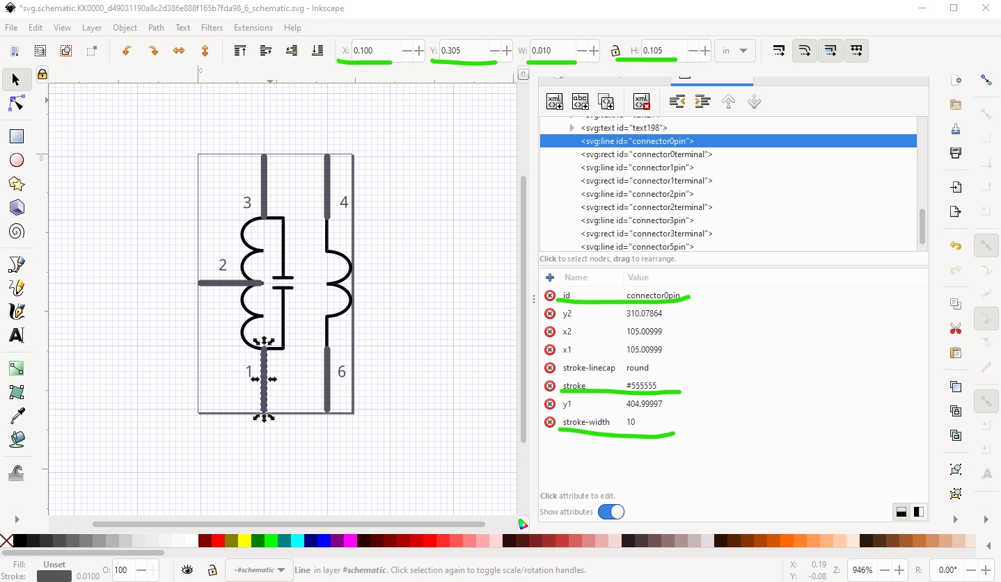
Then I selected the associated line
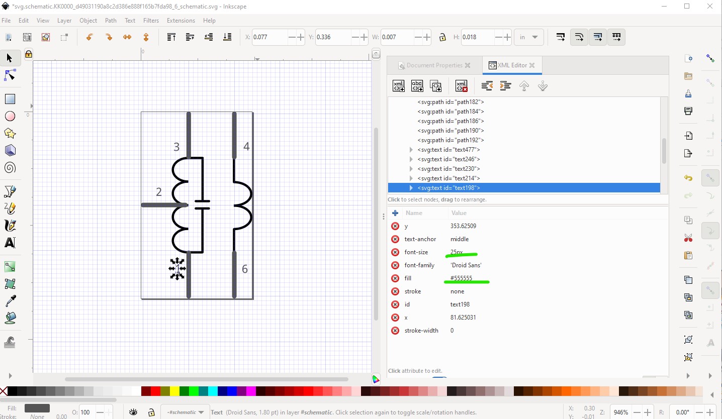
and set the width to 0.1in and height to 0.105in and positioned it at x 0.1in y 0.305in, then changed the width to be 0.1in and the stroke to be #555555 (which is the color specified in the graphics standard for pins.) Next I moved on to the text associated with the pin.
Here I rotated the text to be upright, changed the font-size to 25px (the size for pin labels in the graphics standard) and fill to #555555 (the color specified in the graphic standard.) That produces this schematic svg

which when replaced in your part and run through FritzingCheckPart.py to clean up the pxs in the font-size and check the part. That turns up the following additional errors:
Error 69: File
‘svg.breadboard.KK0000_d49031190a8c2d386e888f165b7fda98_6_breadboard.svg.bak’
At line 9
Found a drawing element before a layerId (or no layerId)
Error 18: File
‘part.KK0000_e983535c73d542d6f35a90388924fc46_9.fzp.bak’
the breadboard svg lacks a layerId corrected by changing layer1 to breadboard in the breadboard svg.
to
and
Error 18: File
‘part.KK0000_e983535c73d542d6f35a90388924fc46_9.fzp.bak’
Connector connector0terminal is in the fzp file but not the svg file. (typo?)
svg svg.pcb.KK0000_d49031190a8c2d386e888f165b7fda98_6_pcb.svg.bak
Error 18: File
‘part.KK0000_e983535c73d542d6f35a90388924fc46_9.fzp.bak’
Connector connector3terminal is in the fzp file but not the svg file. (typo?)
svg svg.pcb.KK0000_d49031190a8c2d386e888f165b7fda98_6_pcb.svg.bak
which indicates there are unneeded terminalIds in the .fzp file. Since they won’t hurt anything (they will be ignored when they aren’t found in the svg) I chose to leave them in.
Warning 14: File
‘part.KK0000_e983535c73d542d6f35a90388924fc46_9.fzp.bak’
At line 127
terminalId missing in schematicView (likely an error)
which indicates the fzp file doesn’t have terminalIds set in schematic which will be a problem with the schematic pins being 0.1 in long! So add terminalIds to the .fzp file like this:
    <schematicView>
      <p svgId="connector5pin" layer="schematic"/>
    </schematicView>
to
    <schematicView>
      <p terminalId="connector5terminal" svgId="connector5pin" layer="schematic"/>
    </schematicView>
which corrects the problem and produces this schematic which is correctly aligned on the 0.1in grid with the wires terminating at the terminalId (rather than in the middle of the pin) like this
from this part
42IF101 IF TX improved v3-fixed.fzpz (6.6 KB)
which has all the above changes in it.
Peter
Hello Peter
Thanks for your efforts. I’m working on a iMac at the moment. When attempting to run FritzingCheckPart I’m receiving an error that an lxml module is missing.
Rather than mess with the Mac (unless there is an easy fix), I will install python on a windows os pc I have - for parts checking prior further uploads. The Mac is running Big Sur V11.6.
All the best.
KingKappa
I don’t use Mac, but lxml is a python library. You should be able to install it from a terminal window with pip install lxml
Thanks microMerlin
This finally worked for me (note I don’t know enough about pip or python if you have issues when attempting this!)
At the terminal
sudo python -m ensurepip --upgrade (return)
sudo python -m pip install --upgrade pip (return)
sudo python3 -m ensurepip --upgrade (return)
sudo python3 -m pip install --upgrade pip (return)
pip install lxml (return)
Then still at the terminal
./FritzingCheckPart.py “if tx_schem.svg” (return) from inside the directory with FritzingCheckPart.py and the svg file you wish to check.
The quotes are used as there is a space character in this particular example svg file.
It works for me on BigSur 11.6
All the best
KingKappa