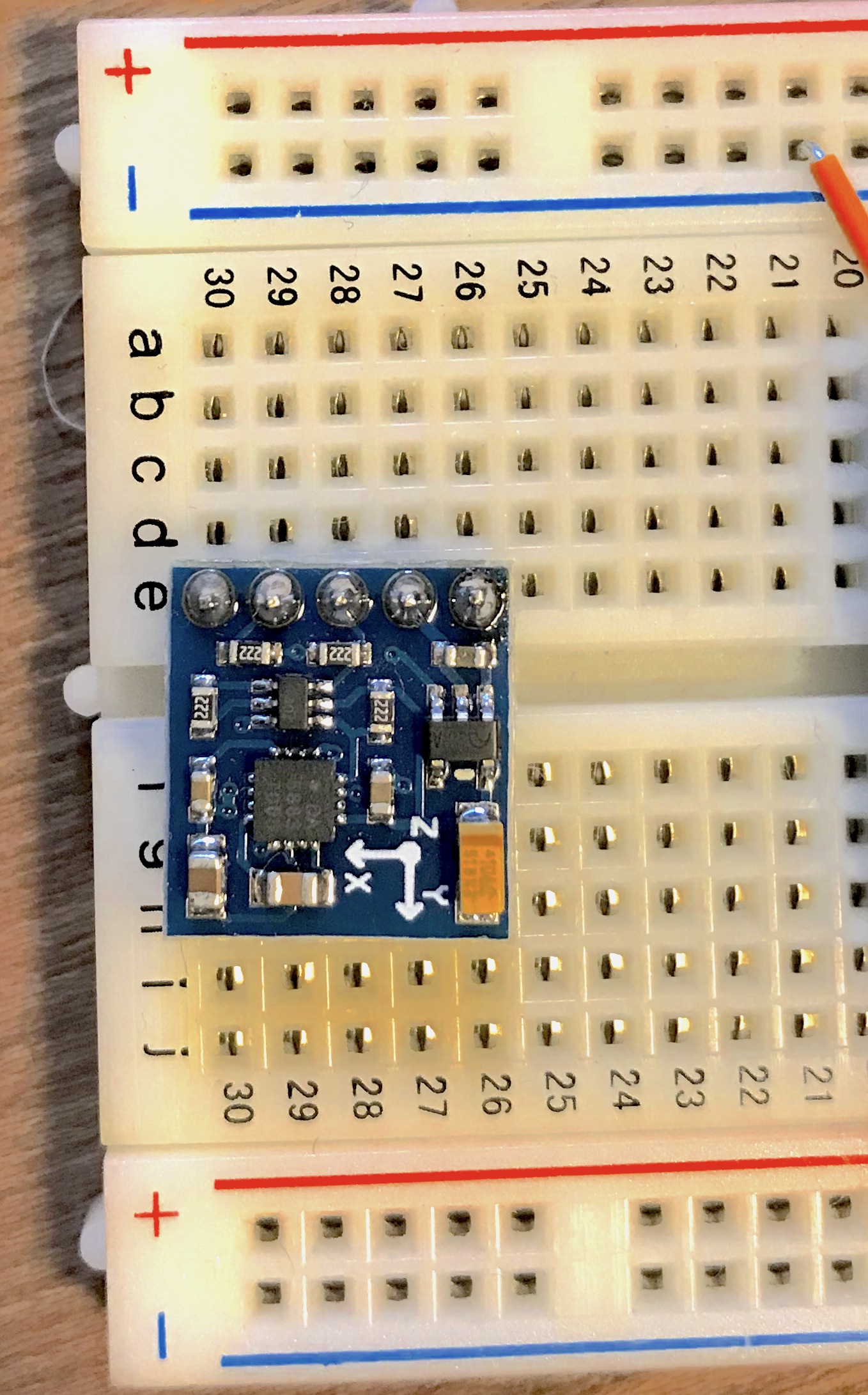
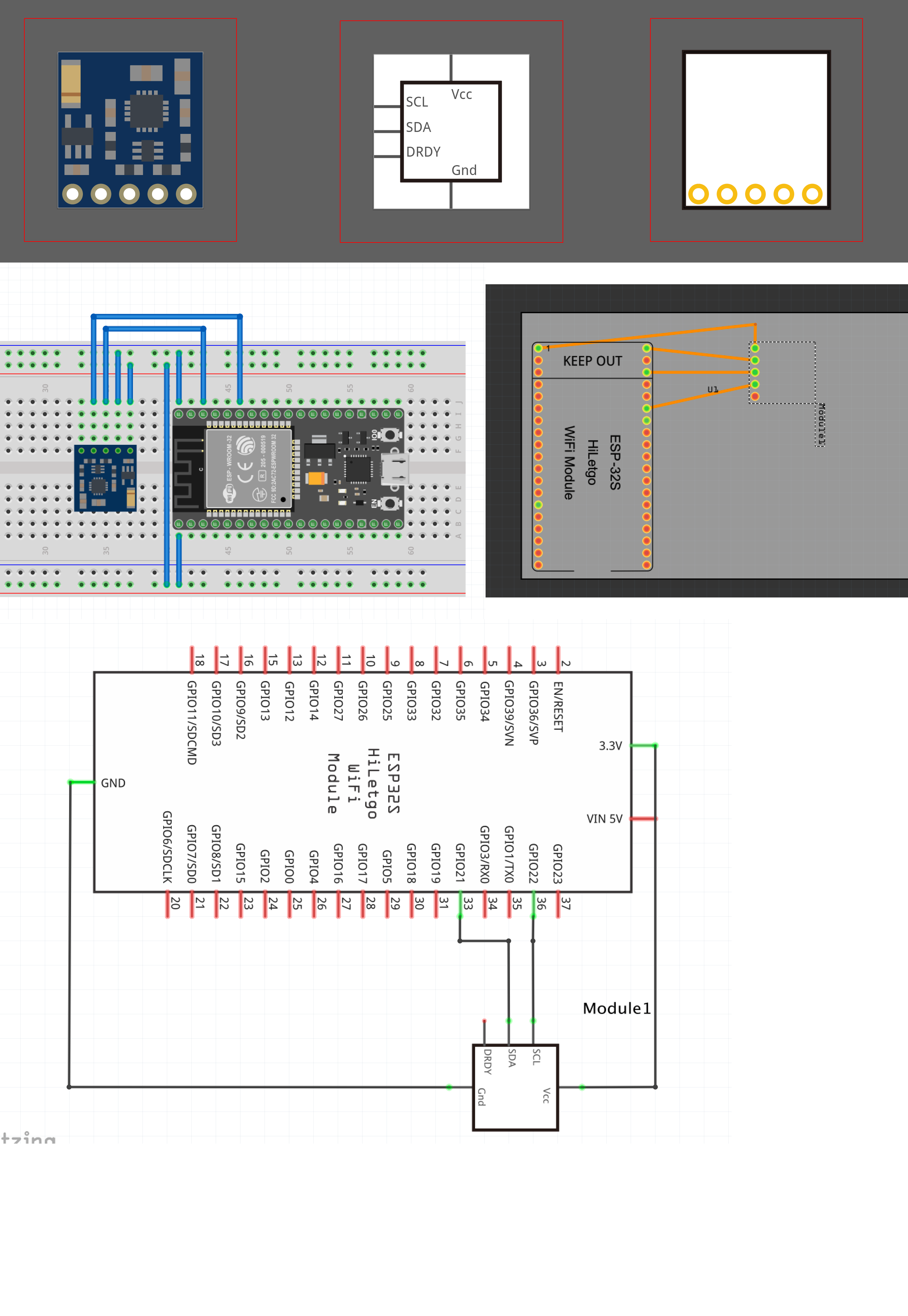
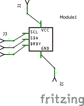
mounted on cheap HMC5883L breakout board.
Like Boladge digital compass module.
(update 05/24)
Boladge HMC5883L Compass Module.fzpz (8.4 KB)
Source Files and new version:
mounted on cheap HMC5883L breakout board.
Like Boladge digital compass module.
(update 05/24)
Boladge HMC5883L Compass Module.fzpz (8.4 KB)
Source Files and new version:
Do you have a picture or link to the real part? Since the ones that I found on google are slighty different from yours.
I asked it because there are “breakout board” variant for the same module. In this case, the one you posted could be named 3-Axis Compass GY-271 HMC5883L.
More info: Arduino Forum
By the way, pretty nice one  Can I upload it to fritzing after waiting for @vanepp part checker?
Hi, thanks KingDarBoja,
Renamed this topic title and I that it is mounted a different chip.
but one thing I can’t found… what is part checker… any applications or @vanepp 's reply or …
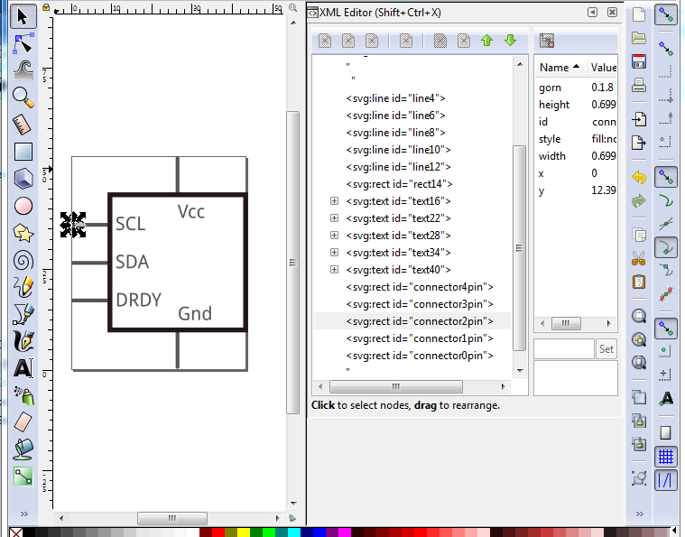
Sorry for the late reply, I have been offline for a couple of months with a broken ankle. The part check script is a python script (available on github) that checks the xml of a part against the parts file format document and reports errors. It isn’t all that easy to use if you aren’t familiar with what a correct part should look like. In the case of your part it (and I) find a number of errors. The svgs are missing layerIds. If the layerid in the svg doesn’t match the fzp file then pdf and svg export on Fritzing don’t work. Breadboard has termanalId specified in the fzp file but not the svg (this doesn’t really affect anything in breadboard), and the same in schematic where it does matter. As well it is desirable to have the outline of the board (so the area it takes up on the pcb is visable during layout) as a silkscreen layer in the pcb svg. This image shows the problems in the schematic svg:
The connection to the middle of the pin (rather than the end which is desirable) is caused by the missing terminalId. I use a 10 thou by 10 thou rectangle labeled connectorxterminal
(where x is 0 to 4 depending on the pin number in this case) aligned to the end of the pin. As well your part isn’t aligned on .1 in boundaries so it doesn’t match with other parts.
Peter
Sorry to too late reply. Please be bless you your ankle. A above image error was fixed in my github repo.
If should upload it here, I will upload a new version.
I tried your check script and then I encountered some warning/errors. But I can’t find those solve solutions in macOS/Illustrator CC’s SVG export.
warning/errors are:
Height 39.49px is defined in px
in or mm is a better option (px can cause scaling problems!)

Width 36.755px is defined in px
in or mm is a better option (px can cause scaling problems!)

Found a drawing element before a layerId (or no layerId)
I am also encounting some drawings are deviated after create a part from svg. I guess it is caused by above warning/errors.
What are you using vector software to edit Fritzing parts?
Thanks to read.
I’m using Inkscape, but if you have and know Illustrator, I’d keep using it. Inkscape has a number of quirks most of which I’m now used to, but any svg editor should do fine. On to your part: my copy of the script (which is a development version not yet released) finds a fair number of errors. Starting with the pcb svg (because that was the last complaint ![]() ), you are missing the silkscreen layerId which is what is causing one of the “Found a drawing element before a layerId (or no layerId)” messages. The first group (Inkscape added a made up groupId, the original file has no id in this group in the xml (as usual I can’t get the forum preformatted text function to work correctly)
), you are missing the silkscreen layerId which is what is causing one of the “Found a drawing element before a layerId (or no layerId)” messages. The first group (Inkscape added a made up groupId, the original file has no id in this group in the xml (as usual I can’t get the forum preformatted text function to work correctly)
< /desc>
< g>
<rect
stroke-width=“1”
fill=“none”
stroke-miterlimit=“10”
width=“36.8”
stroke=“#231815”
height=“39.5”
/ >
needs an
id=“silkscreen” in it to set the layerId correctly.
schematic needs a group with id=schematic (there will be another complaint about drawing element before layerId about that). The terminalIds are still missing as well which will cause the wires to connect in the middle of pin rather than the end. The scale is a bit wrong too. The drawing dimensions are in inches (not px) so that should be OK, but the lines don’t align on .1inch boundaries which will be why it is not aligned with the grid in schematic in Fritzing. You need to move the lines up and for the veritcal ones across so they align on .1 inch boundaries. The you need to add a .01in by .01 rectangle named connector0terminal and position it on the end of the line for the connector. Once you add the rectangle parts editor will put it in the right place with the set the east/west/north/south settings (I have never been able to get it to work and just edit the svg, but other people use parts editor to do this). If you like I can fix the schematic svg up and post a copy so you can see what needs to be done. You have managed to fix the height/ width in px warnings, all the svgs are set correctly in “inches”. The warning is referring to the first element in the xml (this is from schematic):
“svg
xmlns=“SVG namespace”
x=“0px”
y=“0px”
viewBox=“0 0 39.5 39.2”
id=“レイヤー_1”
baseProfile=“tiny”
width=“0.548611in”
version=“1.2”
gorn=“0”
xml:space=“preserve”
height=“0.544444in””
if height said
height=“0.544444”
or
height=“0.544444px”
then you will get the warning and Fritzing may guess wrong and screw up your scale. As I said these 4 svgs are all correctly set to inches and should be fine, other than schematic may have been converted to inches when the scale was wrong, as its scale is currently off.
Peter
@vanepp Thank you for your help and script. I guess it become to perfect !
Boladge HMC5883L Compass Module.fzpz (197.8 KB)
Close but no cigar  , much better but still three issues away from perfection. In PCB your silkscreen, isn’t showing because it is not in group silkscreen. When it is in group silkscreen that group is below copper1/copper0 when it should be above them, and finally the hole in the pin are too large (0.043204 rather than the desired 0.038 for .1 header pins). The hole size calculation is pad diamater in inches (0.078) - 2 * stroke width (where stroke width is 20 when scale is at 1/1000 which your svg isn’t). I was lazy and instead of doing the math, I copied in a proper pad from another part and just copied the parameters in to your pads. Here is a replacement part with the pcb svg fixed up. It has the same moduleId as your current part so you would need to unload the current part before loading this one (or just unzip it and see what I did to the pcb svg).
Boladge HMC5883L Compass Module2.fzpz (186.6 KB)
I just noticed the fzpz is huge (186K) That appears to be because there is a font loaded in the schematic svg. It would be better to use OCRA (it will get substituted by Fritzing anyway) and remove the font definition from the svg.
Peter
Boladge HMC5883L Compass Module.fzpz (6.1 KB)
Again I fixed above maybe. One question, Fritzing graphic template looks like wrong hole size, isn’t it?
Better (for starters, size is now 6.2K rather than 200K, but still a few problems
mostly in schematic: ungrouped everything to avoid translates, moved the pins to the associated lines and deleted the circles. Moved the pins to be on .1 in boundaries added 10 thou by 10 thou rectangles for all pins and made them connectorxterminal. Replaced the individual characters in Vcc, SDA and DRDY with a single text string containing all the letters. Both more efficient and easier to place in the svg. Did an edit->resize page to selection to update the viewbox (you should always do this before grouping the final document)
PCB
Changed the pads to be standard 0.078dia with 20 thou pad width to fit a standard .1 header. The calculation in Inkscape is hole size = dia - (2 * stroke-width) but because the document isn’t at standard scale (which I didn’t correct) I copied in a properly sized pad and just copied its style and radius for all the pads.
Fzp file:
Changed type=“pad” to the correct type=“male”, removed the terminalId from all the breadboard entries (they aren’t in the svg) which gives us:
Boladge HMC5883L Compass Module3.fzpz (6.8 KB)
The templates currently have many problems and shouldn’ t be used (they are the wrong scale at 72dpi and sized in px which causes problems for starters). I’m working on updating them and will then see if I can get someone to replace them in the web site.
Peter
Boladge HMC5883L Compass Module.fzpz (6.2 KB)
Again and again, How about this?
Nope, much the same set of errors as before. The complaints about breadboard aren’t serious it will just ignore them but the schematic ones will usually cause the lines to connect at the wrong place.
Error 18: File
‘part.lei_6a28fc466f33fef0e3af4e14a7f87927_9.fzp.bak’
Connector connector0terminal is in the fzp file but not the svg file. (typo?)
svg svg.breadboard.lei_0ece36b00cf4796c2986cb684ae3664a_3_breadboard.svg.bak
Error 18: File
‘part.lei_6a28fc466f33fef0e3af4e14a7f87927_9.fzp.bak’
Connector connector1terminal is in the fzp file but not the svg file. (typo?)
svg svg.breadboard.lei_0ece36b00cf4796c2986cb684ae3664a_3_breadboard.svg.bak
Error 18: File
‘part.lei_6a28fc466f33fef0e3af4e14a7f87927_9.fzp.bak’
Connector connector2terminal is in the fzp file but not the svg file. (typo?)
svg svg.breadboard.lei_0ece36b00cf4796c2986cb684ae3664a_3_breadboard.svg.bak
Error 18: File
‘part.lei_6a28fc466f33fef0e3af4e14a7f87927_9.fzp.bak’
Connector connector4terminal is in the fzp file but not the svg file. (typo?)
svg svg.breadboard.lei_0ece36b00cf4796c2986cb684ae3664a_3_breadboard.svg.bak
Error 18: File
‘part.lei_6a28fc466f33fef0e3af4e14a7f87927_9.fzp.bak’
Connector connector0terminal is in the fzp file but not the svg file. (typo?)
svg svg.schematic.lei_0ece36b00cf4796c2986cb684ae3664a_3_schematic.svg.bak
Error 18: File
‘part.lei_6a28fc466f33fef0e3af4e14a7f87927_9.fzp.bak’
Connector connector1terminal is in the fzp file but not the svg file. (typo?)
svg svg.schematic.lei_0ece36b00cf4796c2986cb684ae3664a_3_schematic.svg.bak
Error 18: File
‘part.lei_6a28fc466f33fef0e3af4e14a7f87927_9.fzp.bak’
Connector connector2terminal is in the fzp file but not the svg file. (typo?)
svg svg.schematic.lei_0ece36b00cf4796c2986cb684ae3664a_3_schematic.svg.bak
Error 18: File
‘part.lei_6a28fc466f33fef0e3af4e14a7f87927_9.fzp.bak’
Connector connector3terminal is in the fzp file but not the svg file. (typo?)
svg svg.schematic.lei_0ece36b00cf4796c2986cb684ae3664a_3_schematic.svg.bak
Error 18: File
‘part.lei_6a28fc466f33fef0e3af4e14a7f87927_9.fzp.bak’
Connector connector4terminal is in the fzp file but not the svg file. (typo?)
svg svg.schematic.lei_0ece36b00cf4796c2986cb684ae3664a_3_schematic.svg.bak
Peter
Boladge HMC5883L Compass Module.fzpz (6.8 KB)
How about this?
Nope same problem, are you trying to do this from the parts editor with the notth/south/east/west stuff? This is why I don’t use it, I can rarely make it work. Here in Inkscape line4-12 need to be the connector0-4pin and the current pins need to be connectorxterminal:
I don’t think parts editor will delete the terminalIds in breadboard, only a text editor on the fzp file will do that as far as I know.
Peter