Hi - A 223p Dual Ganged Variable Capacitor. For your use or modification.
223p Dual Gang Variable.fzpz (12.7 KB)
Improved version
223p Dual Gang Variable.fzpz (59.7 KB)
Cheers
KingKappa
Hi - A 223p Dual Ganged Variable Capacitor. For your use or modification.
223p Dual Gang Variable.fzpz (12.7 KB)
Improved version
223p Dual Gang Variable.fzpz (59.7 KB)
Cheers
KingKappa
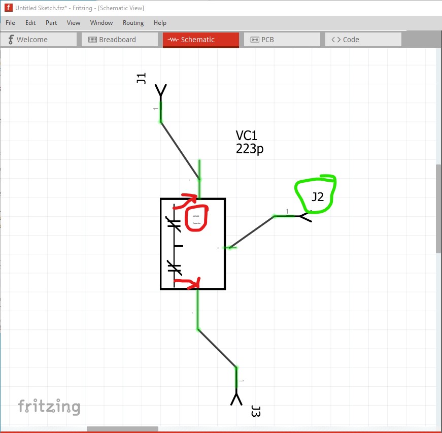
Several problems here. Schematic lacks terminalIds and is thus misaligned (the pins are not on the 0.1in grid) and the fonts likely have px still attached which causes the font size to be too small.
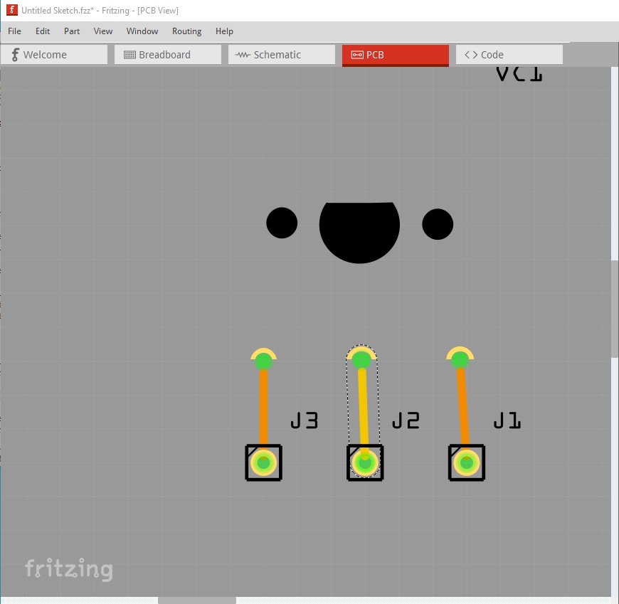
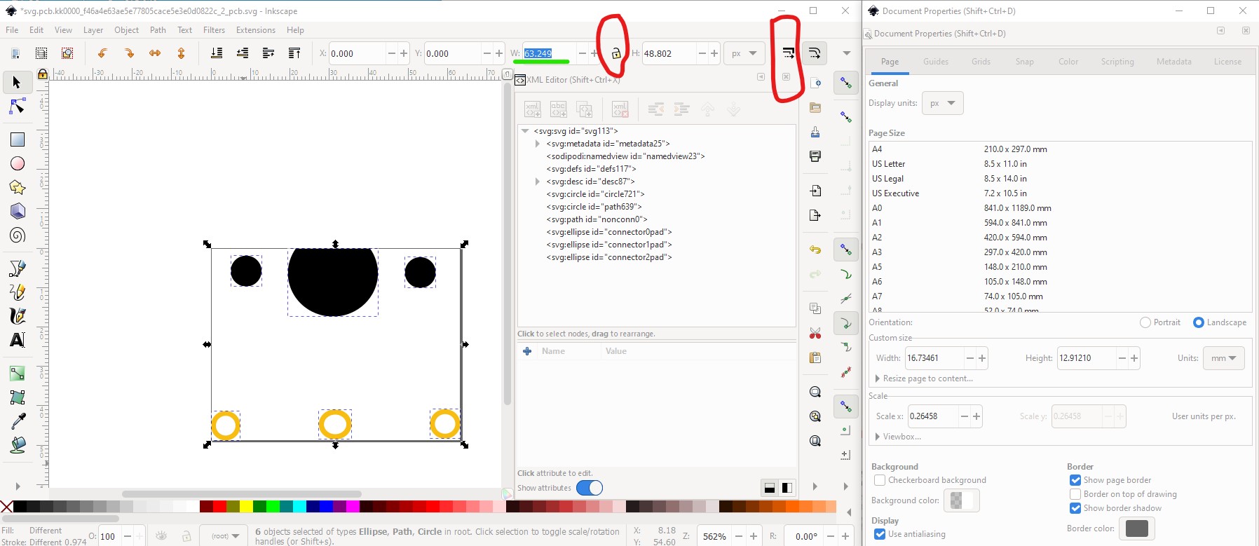
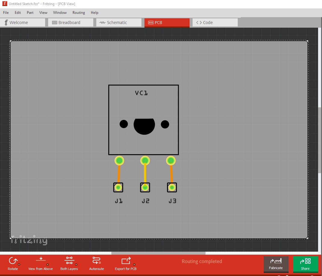
The font in the part (circled in red) should be the same size as the J2 on the connector (circled in green.) The connections to the capacitors should line up with the pins they connect to. In pcb the pads are incorrectly defined somehow (I haven’t yet looked at the svg to see why) and thus don’t generate holes in the pcb gerber export (shown here with gerbv gerber viewer)
Fritzing pcb view (note the half circles!)
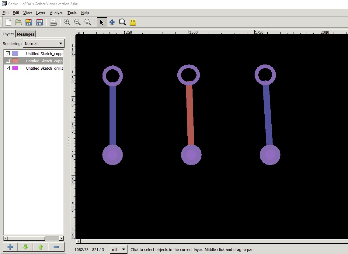
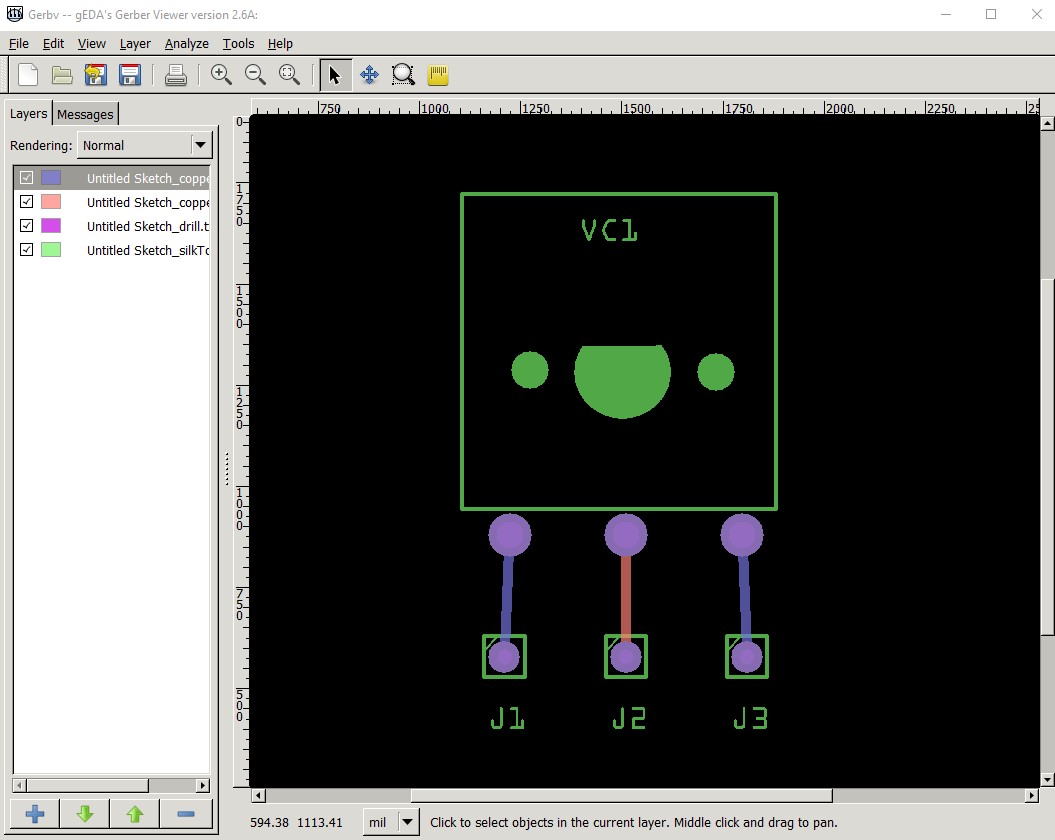
gerbv gerber output. note the capacitor holes have no hole (the purple circle in the connectors below them) and no silkscreen outline of the capacitor body in silkscreen.
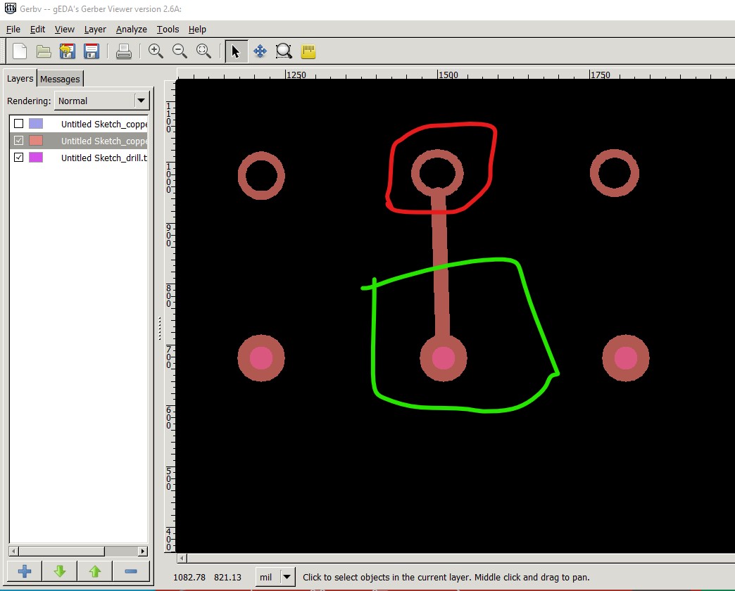
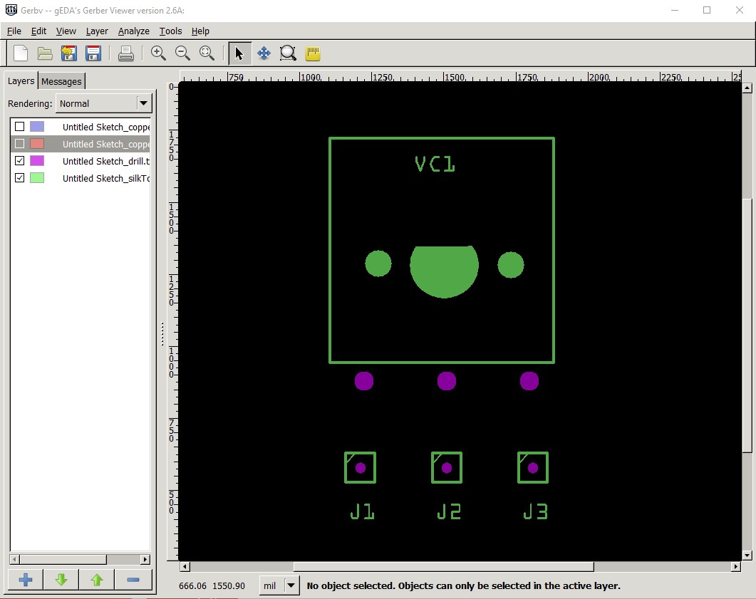
The same view with copper bottom suppressed which shows the hole in the connectors more clearly
the capacitor pins will only get the surrounding pad (which looks overly large as well!) not a hole. I can fix the part up if you like although the data sheets I found don’t give mechanical information so a pointer to a data sheet with pin spacing and hole sizes would be useful.
Peter
Hi Peter - Thanks for the reply and having a look at the submitted part - for comments.
As this is my first journey into Vector graphics, it doesn’t surprise me there are issues - which I will look further into. More viewing to your tutorials required when I get time.
The only data found for this older component is at this URL.
223P Information/Data
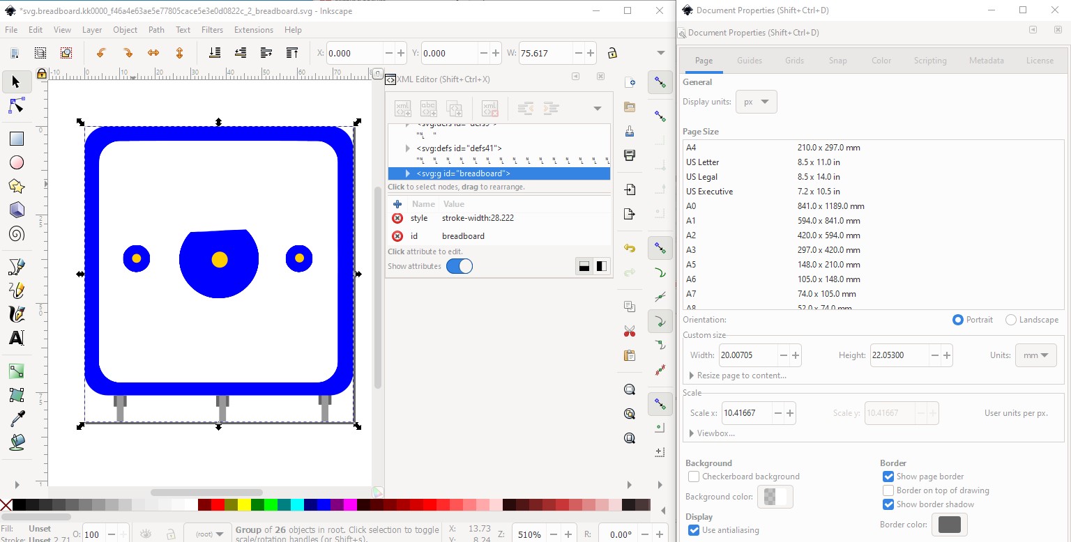
I’ve noticed that Inkscape seems to insert a lot additional information into the tags when the svg file is created. When the pcb svg file is created and imported - the part editing always falls over (copper 0 and copper1 error - even though I follow the layer layout/sequence as viewed from other svgs). I then have to resort to editing the svg in a text editor. Is there a preferred Vector app for creating the svg’s?
All the best
kingkappa
Hi
An improved version. Comments please. Template used for PCB and Schematic.
223p Dual Gang Variable Improved.fzpz (12.9 KB)
All the best
kingkappa
Sorry! Finishing this took longer than I expected. this is based on one of your earlier parts!
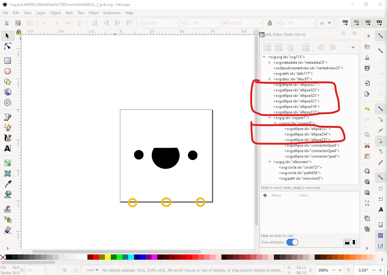
I use Inkscape, because it is open source and free (and thus popular) but any SVG editor will work. Illustrator is a common choice, but as far as I can see from the documentation it doesn’t have a way to set the drawing parameters as Inkscape does. Inkscape just takes some getting used to (and FritzingCheckPart.py to fix some of the incompatibilities with Fritizng such as px on font-sizes!) With that said, lets start with your pcb svg file in Inkscape. There are several things wrong as seen in this image:
the ellipses circled in red can be deleted as they are not needed.
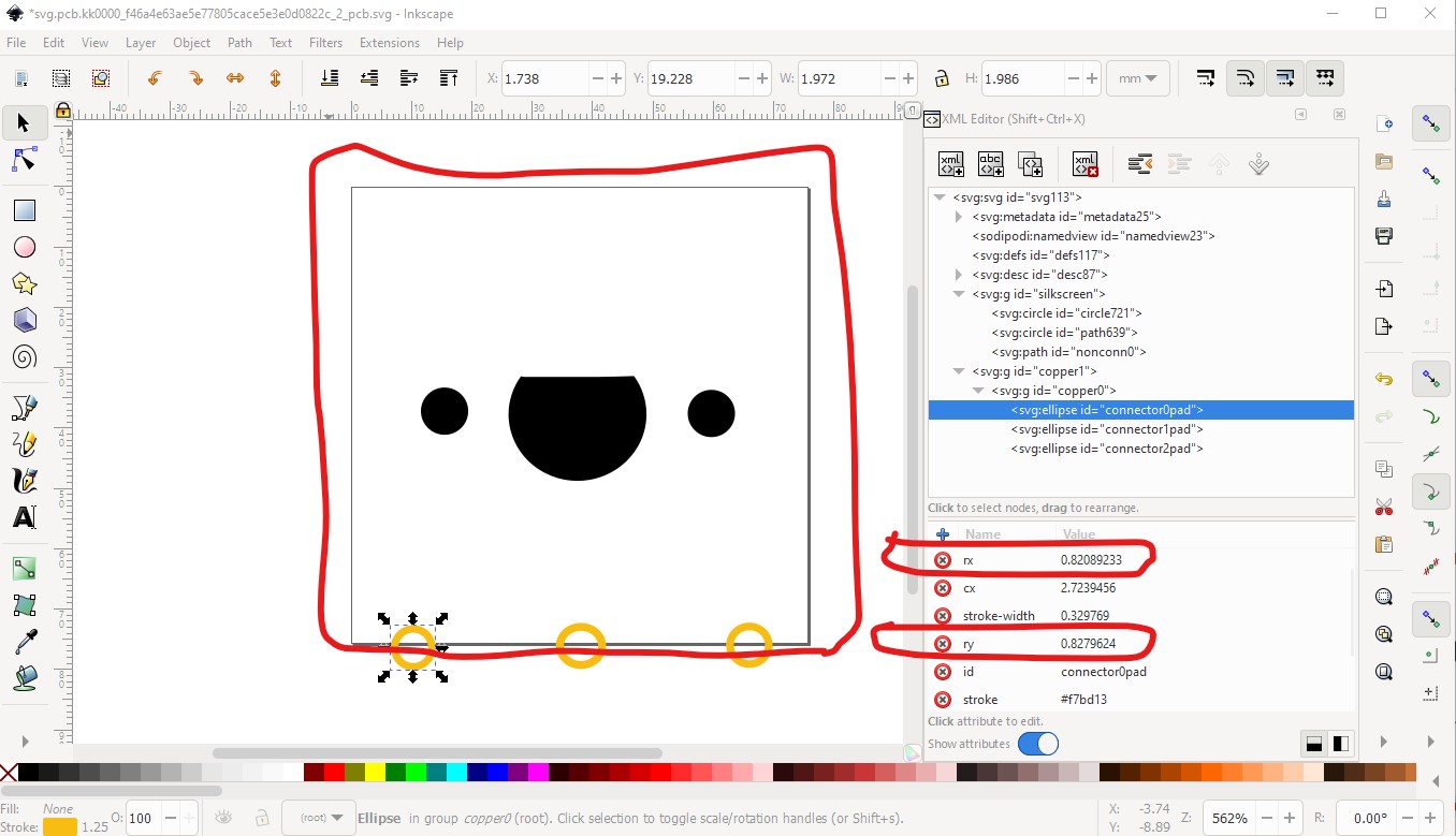
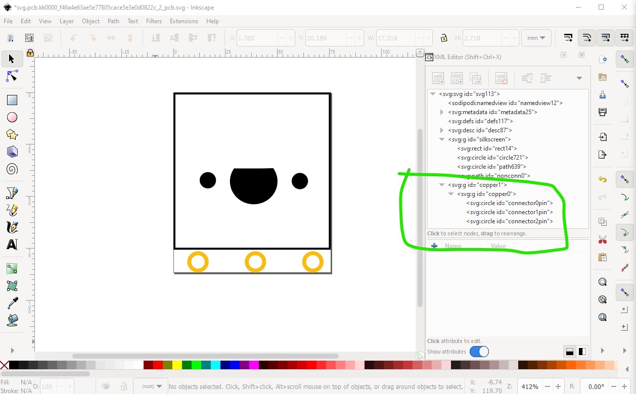
which is the correct format (note I moved the silkscreen group above copper1/copper0 as well) which is still incorrect. The reason the circles are truncated in Fritzing pcb view is the viewbox (the rectangle circled in red above) does not include the full pad and thus the bottom of the pad is truncated (but not in gerber export which is why the pads appear there!) as well the pads are ellipses and the gerber export only creates holes for circles. To fix this I ungrouped everything like this by selecting each group in turn then hitting shift-cntrl-g (ungroup) multiple times to get this:
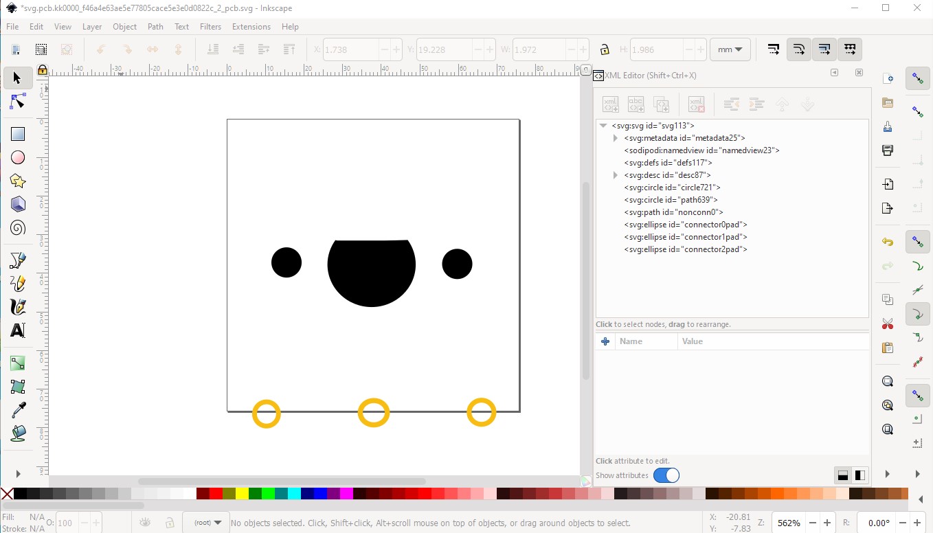
Now I click Edit->select all, which creates this:
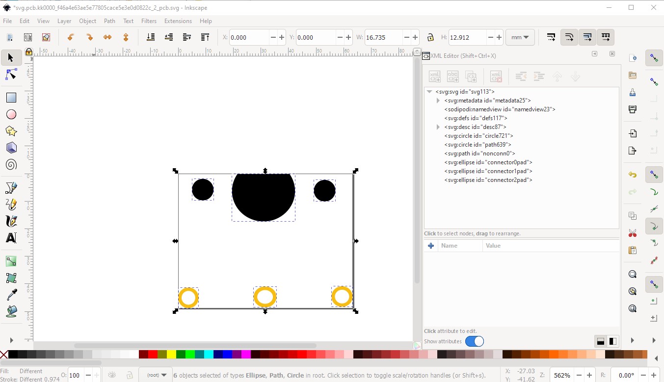
and then Edit->Resize page to selection which resets the view box to include the entire image. You need to do this with the image ungrouped and as the last thing before you redo the groups.
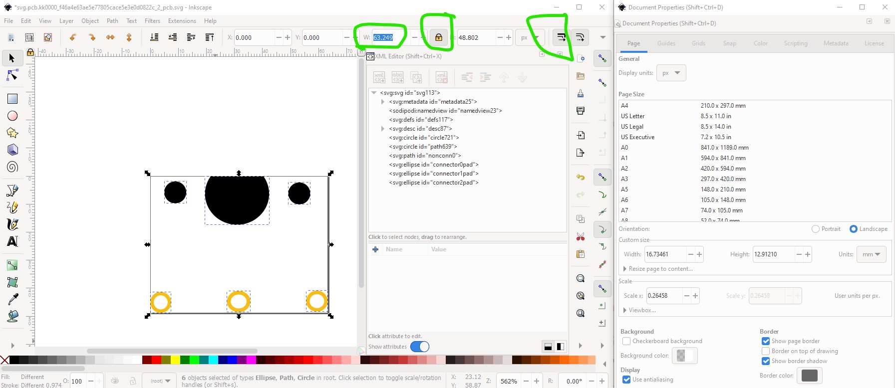
Now I rescaled the image to the desired scale like this (which causes 1 px to be 1/1000 of an inch.) First record the current width from the tool bar (63.249px in this case) then lock the width and height and enable scale stroke width like this:
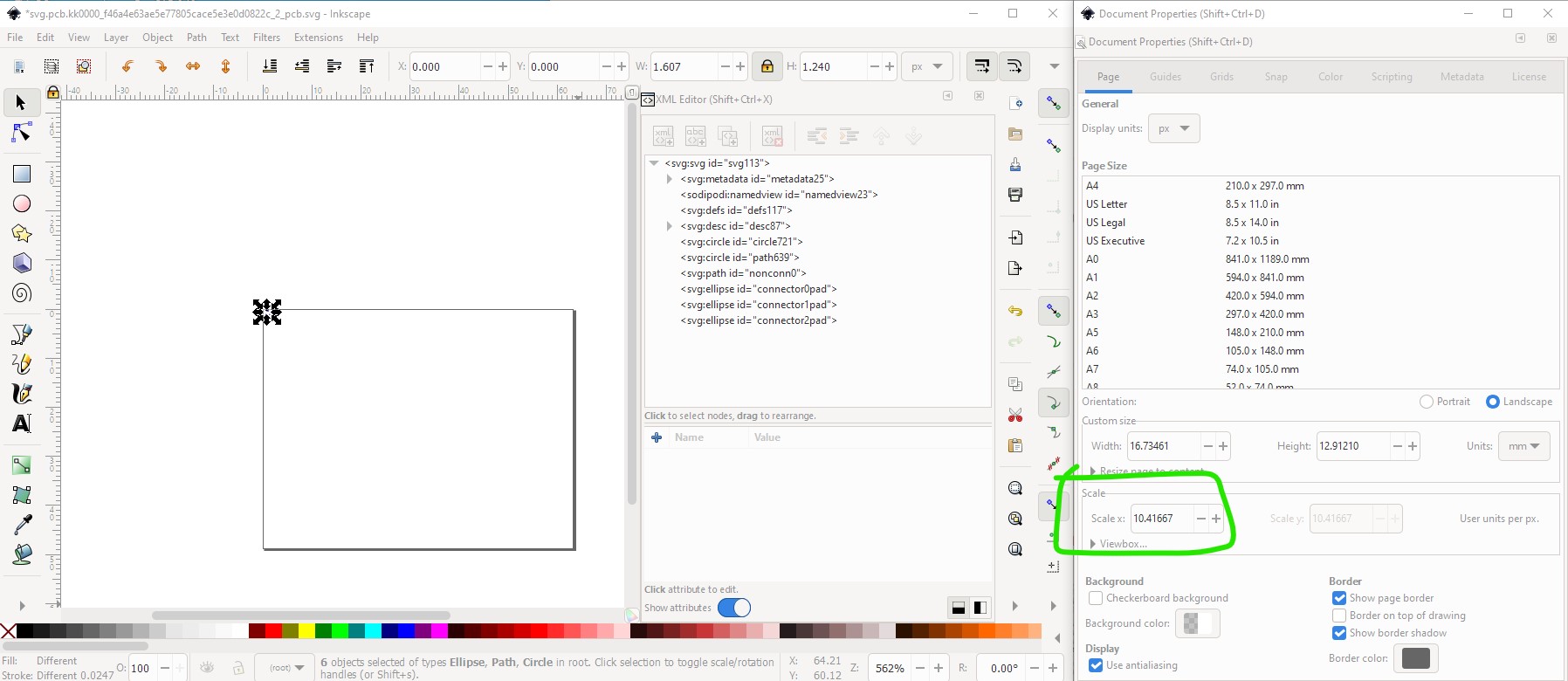
then change the scale from 0.26458 to 10.41667 which makes the image much smaller.
now change the width back to 63.249px to make the image the original size at the new scale. The lock of width to height keeps circles circles (without it floating point roundoff changes them to ellipses!)
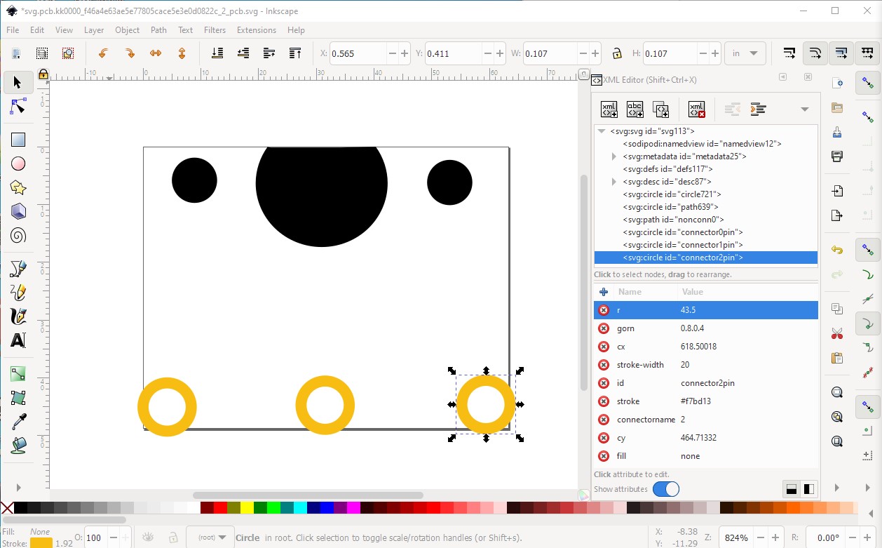
now change connector1pad to connector1pin and adjust it so the hole size is correct. In Inkscape the hole size is calculated via this formula
hole-size = pad-diameter - (2 * stroke-width)
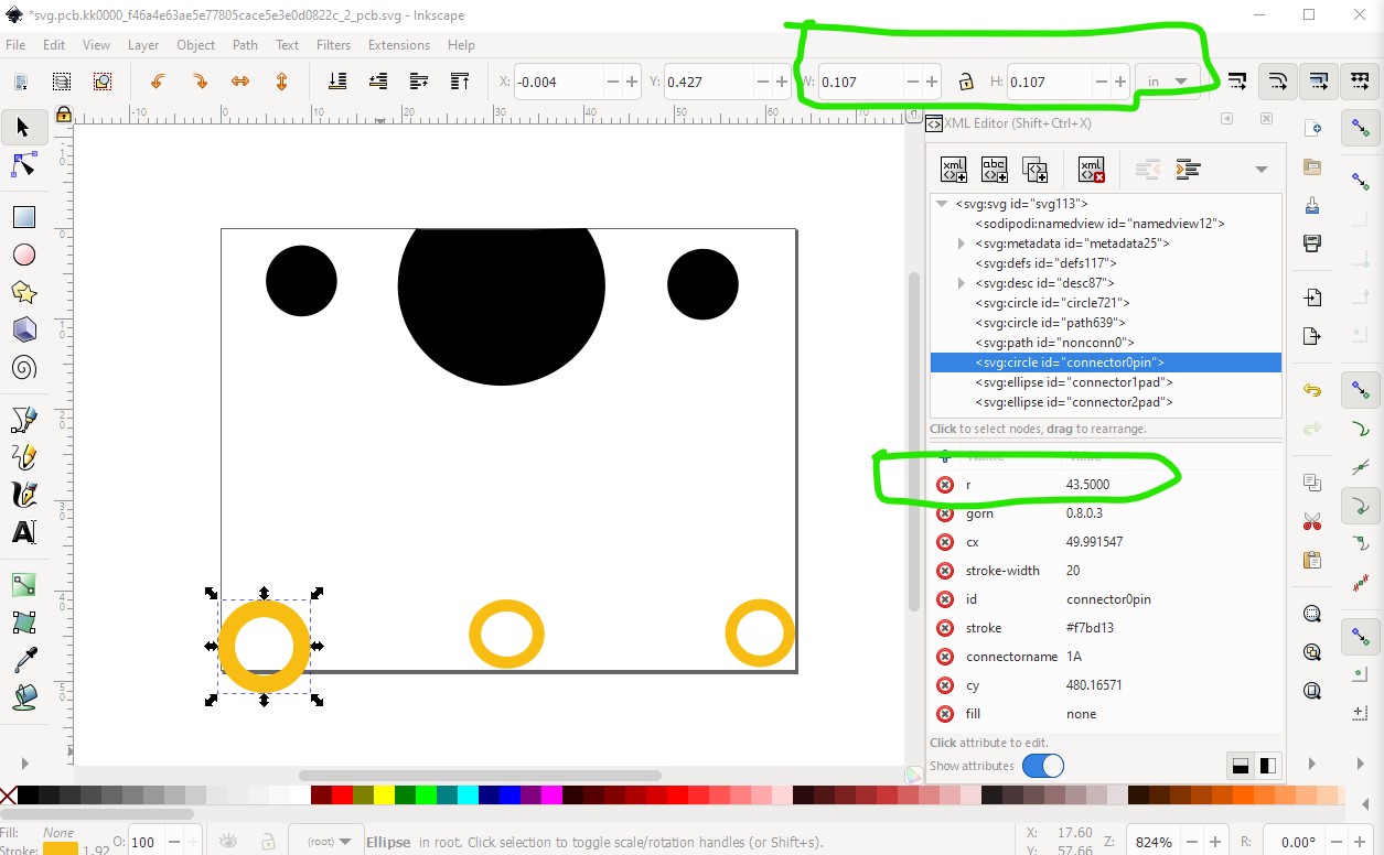
in this case we want the standard 20 thou ring thickness so set the stroke width to 20 to make it 20 thou. From the cap data sheet, the pin is 1.5mm wide so set the hole to 1.7mm (around 0.067in) so pad diameter needs to be 0.107in (0.107 - .40 (2 *20thou).) So set the tool bar in to in, and change the width and height of the pad to 0.107in like this
Note the radius has changed from rx and ry to r = 43.5 making this a circle not an ellipse and it will thus drill a hole. The downside is that this also changed the x/y position of the pad, making it out of place. So undo both the last steps to get back to the original pad like this.
then instead of changing the pad size in the tool bar, set rx and ry to 43.5 like this
this has the effect of updating the circle (or ellipse in this case) in place without moving it in x or y as changing the width and height in the tool bar does. It is however still an ellipse, so select the pad and move it back one position in x like this
this causes Inkscape to convert the ellipse back to a circle (with a single r=43.5 radius) which will drill a hole. So now move it the other way in x to restore its original position. Then do the same thing to the other two pads like this (move each of the pads one step left then one step right to cause them to become circles as well)
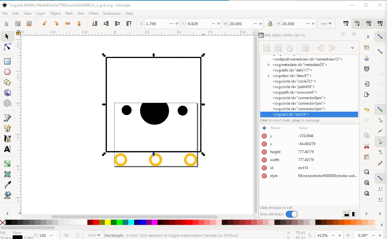
Now do an Edit->select all and Edit->resize page to selection to reset the view box. Connector0 is now x 0 y 10.560mm but connector1 is x 7.239mm (and needs to be 7.3mm) y 10.476mm (needs to be 10.560mm) and connector2 is x 14.605mm (needs to be 14.6mm) y 10.445mm (needs to be 10.560mm) so fix all of those. Then make a 20mm by 20mm rectangle (to indicate the position of the body of the cap!) and place it to give the final pcb layout before grouping.
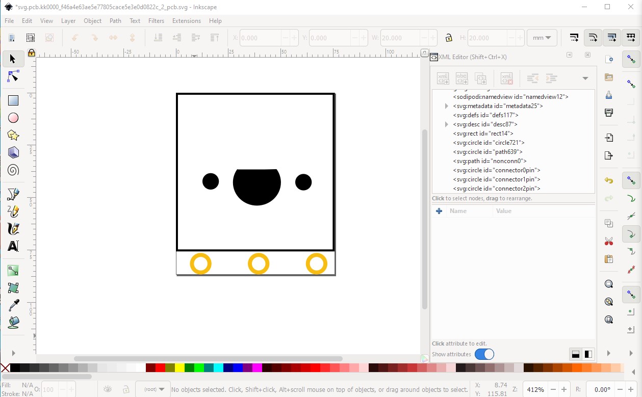
Now do an Edit->select all and Edit->resize page to selection to reset the view box
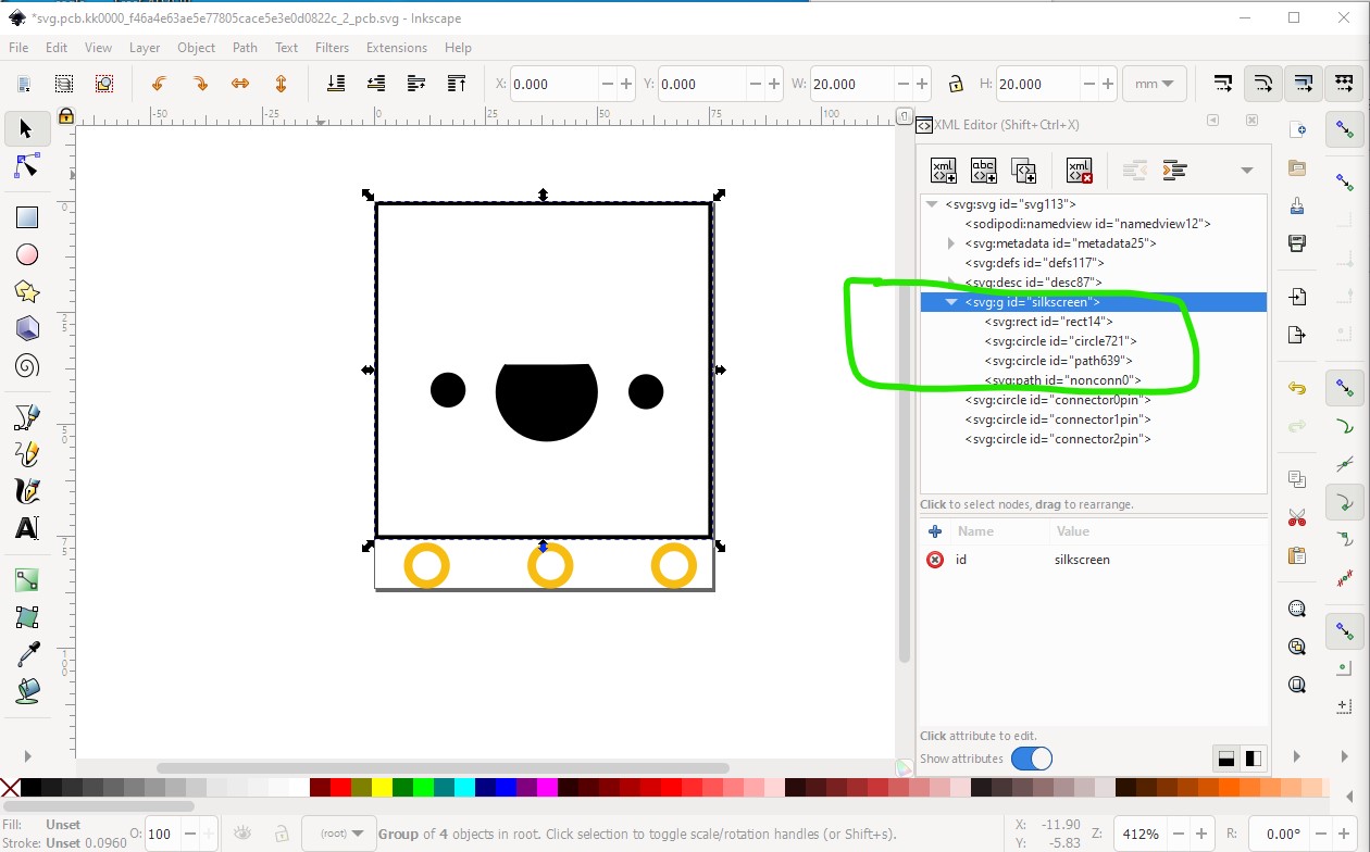
then remake the groups First select all the silkscreen and group it.
then group the pads twice to make copper1 and copper0
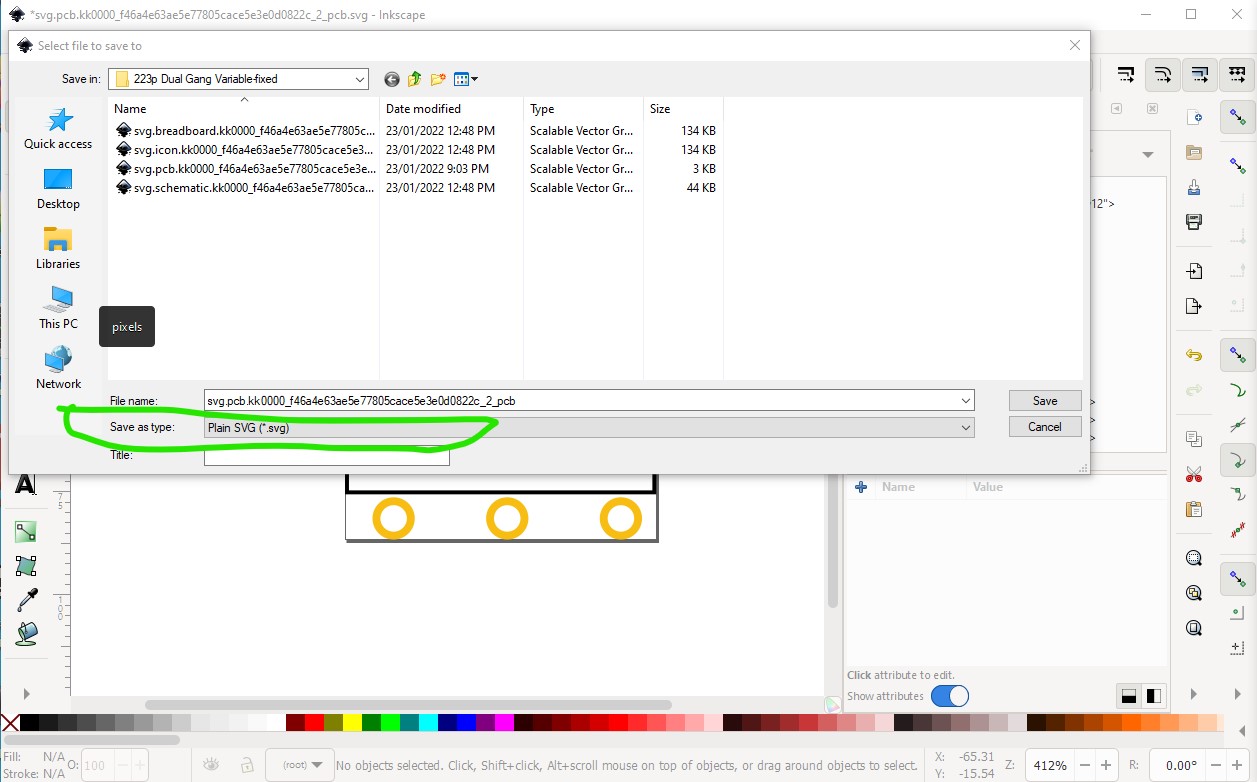
Now the breadboard svg is done so we need to save it. To avoid the extra Inkscape metadata (which sometimes irritates Fritzing) instead of using save, use save as and select palin svg like this
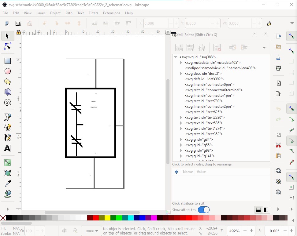
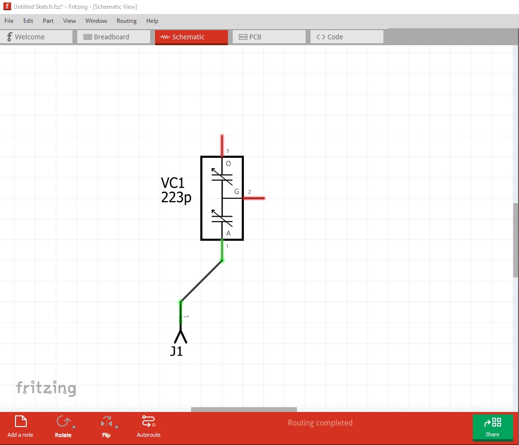
now on to schematic. The first problem is that it lacks a layerId.
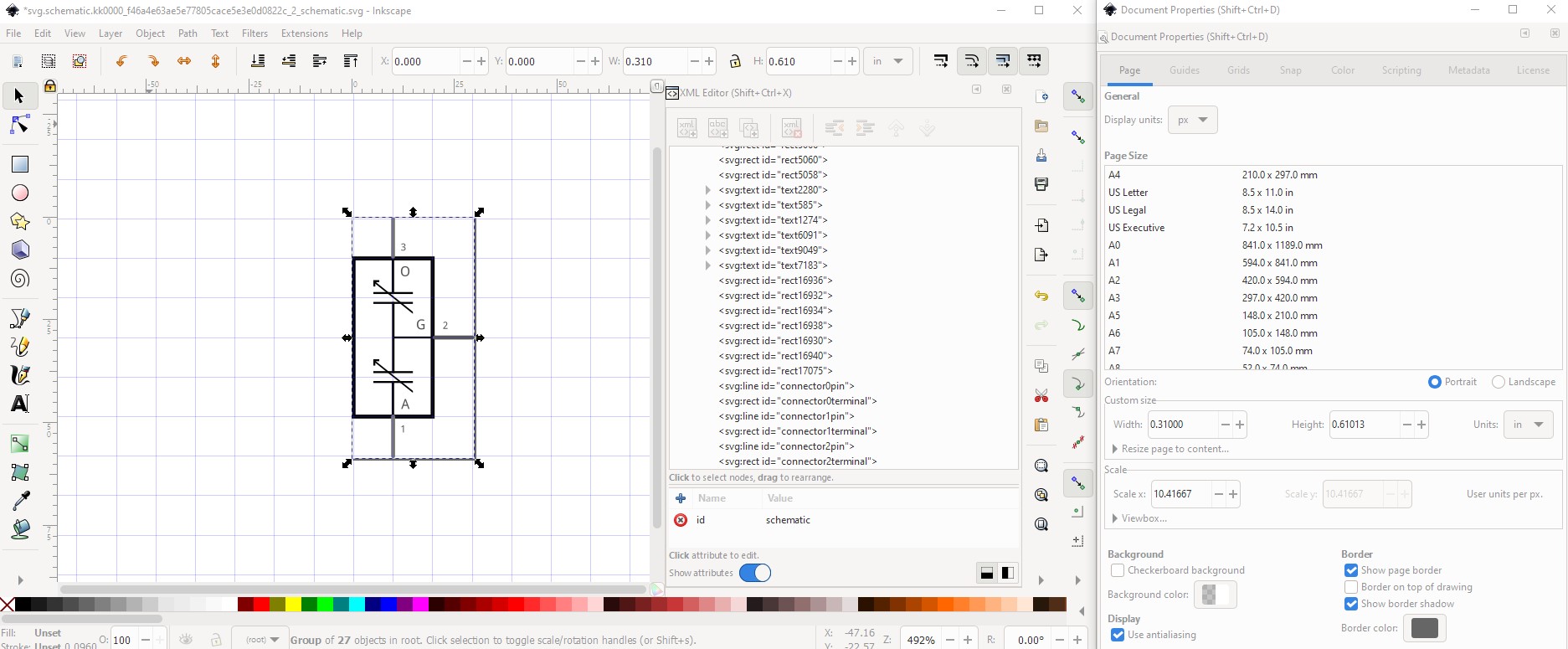
to create one you need to do an Edit->select all then Object->group and name the resulting group schematic. However more things need to be done first so ungroup everything and rescale the svg as I did in pcb. Then reduce the size of the pins to 0.105in and change the color to #555555 as specified in the graphic standard, set the stroke width to 10, then repeat for the other 2 pins. Reduce the size of the rectangle to make the part as small as possible. Remove the Variable Capacitor text as it doesn’t easily fit (and needs to be 60px font size in the graphic standard which makes it too big!) Do Edit–>select all, Edit->resize page to selection, Object->group and set the group name to schematic to set the correct layerId and schematic is done.
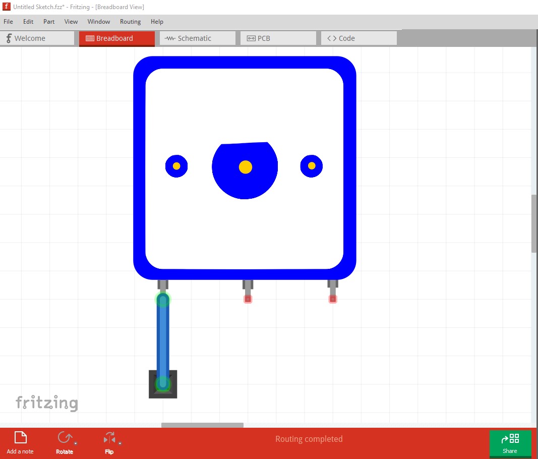
on to breadboard. Again no layerId (without the layerId the part will not be exported to an image such as svg, jpg, png etc.) The scale also isn’t correct so ungroup the svg and rescale it. Move the connectors on to 0.1in boundaries, and replace the connectors with a square at the bottom of the pin. Then Edit–>select all, Edit->resize page to selection and Object->group and name the group breadboard to create this
on to the fzp file
reuse the breadboard svg as the icon svg
<iconView>
 <layers image="breadboard/kk0000_f46a4e63ae5e77805cace5e3e0d0822c_2_breadboard.svg">
  <layer layerId="icon"/>
 </layers>
</iconView>
this eleminates the need for the icon svg. Change the pad in the pcb connectors to pin as this is a through hole part not SMD. Add the url to the datasheet.
<url>http://www.hdic.com.hk/?topclassid=11&classid=204&id=761</url>
note you need to escape the & in the url with &
and we are done. Now run the result through FritzingCheckPart.py to make sure all is well (note this is a newer version than the released one!)
$ FritzingCheckPartw.py part.kk0000_5cebc0864f45da596ed68db5df518fbf_2.fzp
File
‘part.kk0000_5cebc0864f45da596ed68db5df518fbf_2.fzp.bak’
This is a through hole part as both copper0 and copper1 views are present.
If you wanted a smd part remove the copper0 definition from line 39
Modified 1: File
‘svg.schematic.kk0000_f46a4e63ae5e77805cace5e3e0d0822c_2_schematic.svg.bak’
At line 119
…
(notification that it removed the px from the font-sizes)
Removed px from font-size leaving 25
Modified 1: File
‘svg.schematic.kk0000_f46a4e63ae5e77805cace5e3e0d0822c_2_schematic.svg.bak’
At line 131
Removed px from font-size leaving 25
but otherwise fine. So now use 7zip to zip the fzp and 3 svg files in to a .fzpz file
then load the new part in to Fritzing (you will need to delete your old part first as I didn’t change the moduleId!) and test it. Connect the pins one at a time, then make sure they connect where you expect in all views.
breadboard
schematic
note the offset of the header makes sure the terminalId is connecting correctly to the end of the pin!
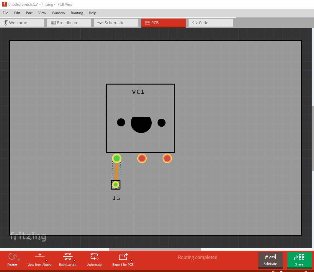
pcb
now repeat all the other pins. In pcb move at least one trace to the top layer to make sure both layers work,
then export the sketch as gerber files via
File->export->For production->Extended Gerber (PS-274x)
then edit the resulting drill.txt file and check the hole sizes are as expected.
; NON-PLATED HOLES START AT T1
; THROUGH (PLATED) HOLES START AT T100
M48
INCH
T100C0.038000
T101C0.067000
%
here the headers are 0.038in and the cap holes are the expected 0.067in and thus all is well. Now load the gerbers in to a gerber viewer (this is gerbv) and check everything is OK (gerber processing happens after the display of the image in pcb view and can have problems that don’t show up in Fritzing!)
here I surppressed the copper layers to see the drill holes
all looks to be well so the part is complete. Here is the fixed up part
223p Dual Gang Variable-fixed.fzpz (32.1 KB)
that created the above images. Hope this helps!
Peter
Hello Peter - Thanks for your efforts and detailed explanation provided. Plenty of information to digest and Vector graphics skills to improve.
I’ve slightly modified the PCB View as I was not happy with initial image and think it is better and closer to the device specifications.
223p Dual Gang Variable_fixed_plus.fzpz (62.6 KB)
All the best
kingkappa