Hello all,
I wondered if there’s a best way to layout two PCBs in the PCB view so that when you send it off for Fabrication, say to Aisler for example, firstly is there a way to do that in Fritzing (I found slightly overlapping two boards means Aisler complains that there is no outline border), I was going to overlap them and then place some non-plated holes between them, but so far it looks like that won’t work, so I’d love to know the best and easiest way to this (i.e. I don’t want to design a special PCB which has both PCBs in it’s SVG design, but if that’s the only way then I’ll have to consider it).
Thanks, James.
I assume that what you want to end up with is 2 pcb boards, but have fabrication see it as one combined pcb that you will cut apart after you get it.
The only way I see to do that, is to make a single larger board in Fritzing. Since the 2 boards probably do not have a common dimension, where a larger rectangular board would get what you want, you need to create an svg file with the desired “L” shape, and import it to the pcb part (in inspector). You might get away with creating that shape with only a narrow channel connecting the 2 pieces, to make the separation simpler.
That is going to involve some extra work. I expect you want to do the initial layout using 2 separate board in Fritizing, then combine them after you know the exact dimensions of both boards. If you are careful, you should be able to create the empty combined board, then drag select everything on the other boards (one board at a time), and move it to the new board. Locking the original pcb board, but making sure all of the parts on it are not locked should make that simpler. The parts will move, but not the pcb itself.
See this page for basic information on creating a custom board shape. I am used to xml / svg, so for that simple of shape, I would just create it manually in a text edit using the dimensions I wanted. As usual, check the gerber output before sending it off to fabrication.
I’ve posted too many How-To-Do-It’s on making custom PCB shapes (including cutouts and V-groves) using various Graphic programs and by Homemade SVG’s. It’s gotten too cluttered and probably confusing by now.
However, what you want is extremely simple.
This Youtube vid will help to understand.
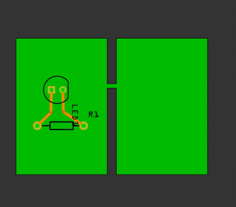
This post shows concept of PCB with break-away PCB’s.
Thus, Make a PCB with as many break-away sections as desired.
Copy your circuit (from desired PCB) and Paste the circuit on desired break-away section.
Example below
Thank you very much.
Unfortunately the placement of the parts has to be very exacting to get the GPIO pins in the correct spot to align with the mounting holes. That’s why I was hoping there would be a way to add two PCB boards (SVGs) to one fritzing and have them joined only in fritzing.
What I’m doing currently is making one SVG with the board and the GPIO pins, then I expport two different SVGs, one for the board, and one for the pins (and holes), then set their location to the same position in fritzing to be sure they line up as designed.
Thanks anyway for your help guys!
James.
I won’t belabor this - just final comment’s:
• Perhaps I’m missing the point but, I assume you want Two PCBs that, if stacked on top of one-another, all Holes/etc will line up.
And, that you want to save costs by having two PCB’s in one process-job.
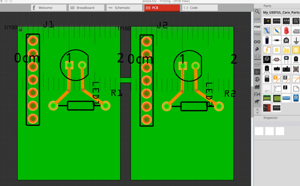
• Whatever the two PCB shapes and dimensions are, you can place the PCB’s, parts, pads, pins, etc, Exactly where you want them on each PCB.
Use the Ruler Part to help (shown in image below). Thus, the Dimension’s of segments connecting the two boards is only important to your needs and the PCB vendor’s prefferrence (some do V-cuts, some do Mill routing and some do Laser and Water-Jet cutting. Check with Vendor).
After knowing about handling Two connected PCB’s, position the stuff as needed using the Ruler Part… There’s also the Cursor Position Info at the bottom the PCB panel.
I do this quite often (I CNC mill my PCB’s). You can see from the Ruler Part that all Parts and Pads/Holes are at same relative position on PCB’s.
The exported Gerber’s contain the correct dimensions.
Thanks for your help, but I think I wasn’t being clear…
I am making a hat for a raspberry pi (project 1).
I am also making another tiny PCB project for a totally unrelated thing.
I want to put them to be together (ideally) only so that they’re sent to the fabrication site that way, then be seperated after, just to save on PCB cost, but I’ll just sink that cost as I think it will be too fiddly.
However if a company like @aisler could do this on their end (i.e. give them two Fritzing projects and they make them together, that would be great). But I imagine something like that isn’t high on their priorities.
James.