Would you upload the sketch (the .fzz file) please? Upload is 7th icon from the left on the reply menu. At a quick look at the svg, it likely isn’t formatted correctly for a custom svg (although I’m not the expert on that either). Hopefully @opera_night who is much better at these will comment. This is usually tricky and hard to get right, although @opera_night has a number of posts on how to do it in the forum. The holes need to be dragged on to pcb layer from the pcb View section of core parts (the right hand window in Fritzing) or specified in the copper1/copper0 layers of a part. You likely want the first option here. I don’t think you can make them as part of the cutout custom svg (but I could be wrong). The keep-out is automatically generated from the parts, it isn’t a specifiable layer. There are tricks you can do with substituting mask layers from different gerbers to make odd mask requirements work, which involve generating a mask that does what you want (usually by removing something from the sketch) then coping the gerber it creates in to the real sketch’s mask gerber file.
Rather than repeating info I’ve previously posted, look at my most recent posts re making PCB’s.
the Upshot:
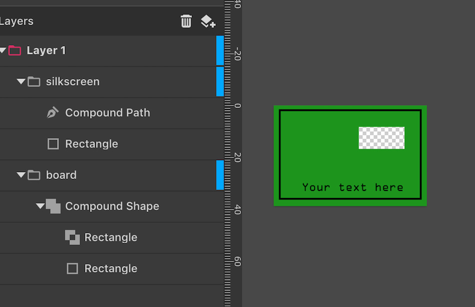
The PCB svg is not the same as a Part svg.
The PCB svg does not have copper layers.
I opened your file and recommend starting over as the time/effort to correct what you have will be inefficient.
Helpful (I hope) is screenshot of a basic PCB svg layer setup… Not important is the ‘compound’ shape (which is just a different word for a Path… Don’t fuss about that. What is important are the Layer names
If you redo it and need further help, having understood my post’s, we’ll have a common foundation of understanding to solve your problem.
And, yes, you can copy&paste elements from your current file into the correct layers in a redo (thus saving about two minutes of work…)
Lastly, the SVG can be made with a text editor (which is all an SVG is, a Text file). Thus, while most all drawing apps that export SVG’s are useable (to certain degrees), they can (and do) add stuff Fritzing can’t handle so, best to keep it simple. Especially for a First-Time. So, make a very basic PCB, after success, get to where you want to be in the next step’s…
[EDIT ADDED] If you’re trying to make a ‘Part’ (Parts have a PCB but, not the Board’s PCB) take a look at most any Part. For ref, here’s my microSDcard part as an example (and Peter has posted many helpful parts to look at) http://forum.fritzing.org/t/micro-sdcard-part/5866/4
Thanks, I redid the design in Illustrator instead of importing a SVG from my cad program and that seems to have solved it!
Just a couple more small things
According to the pi-hat specifications:
I’m not sure if it’s possible to define the soldermask in Fritzing at all, since I can’t add a copper layer in the pcb file I’m not sure how to correct it?
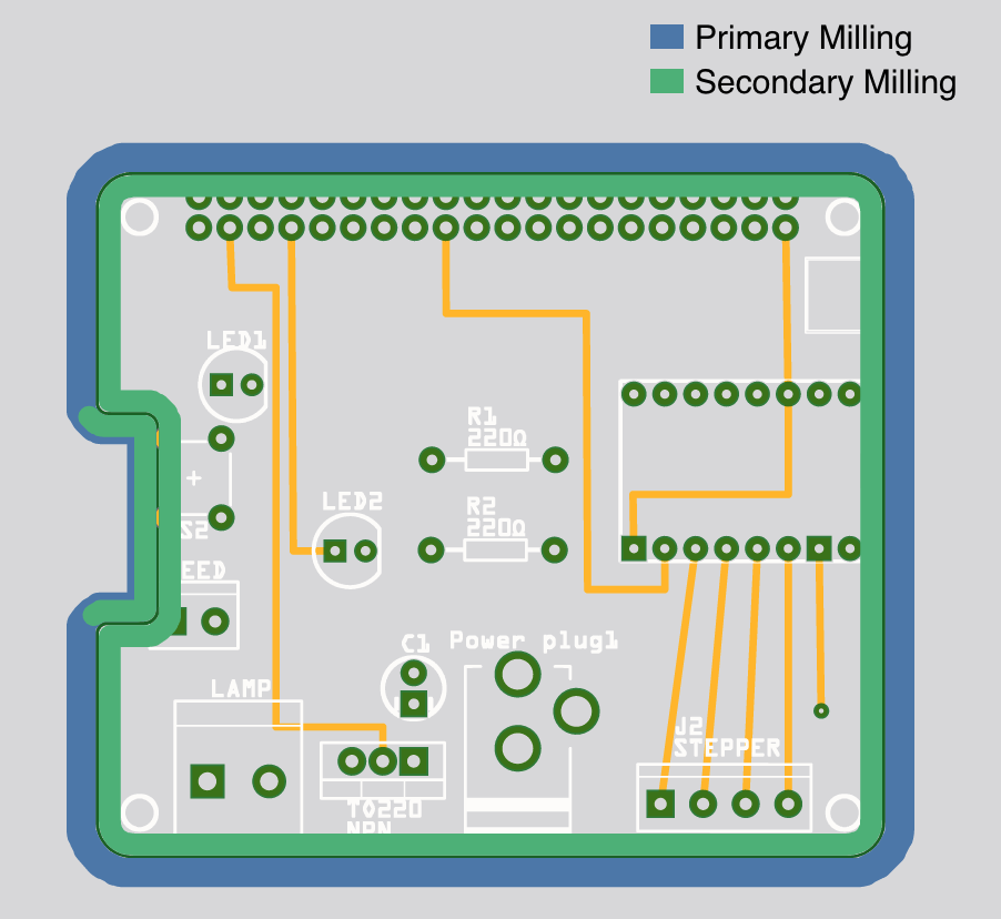
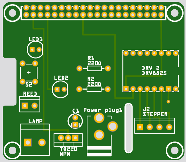
Second problem is the GPIO location, this is where it should be according to the specs: (white box on pcb below)
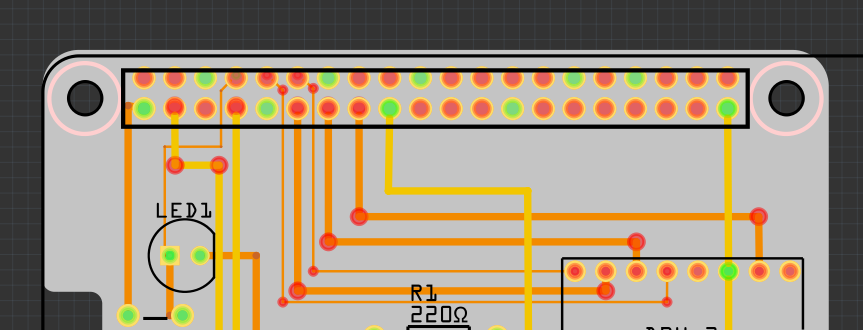
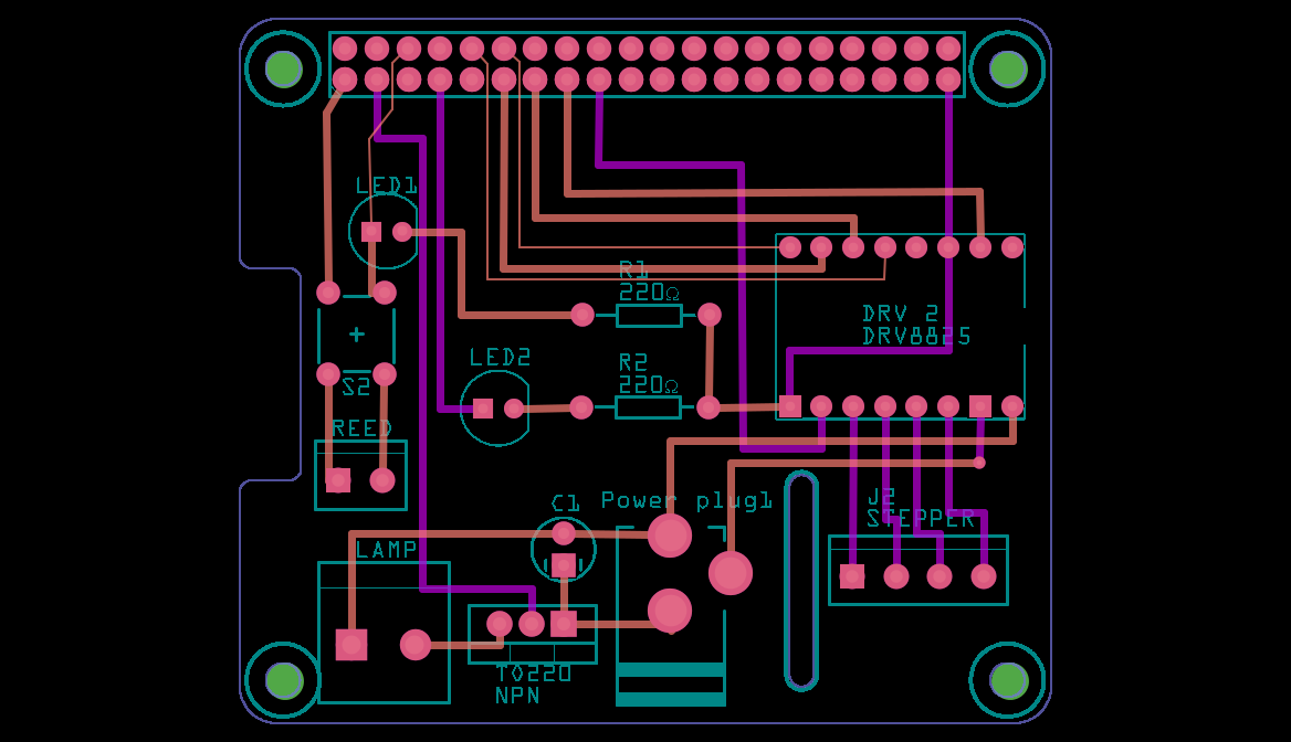
But when I align the holes on the RPI and the custom PCB it looks like the gpio header is a bit off on the render below.
Regarding Soldermask:
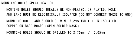
Identify soldermask/ keep-out zones & other necessary features on a PCB drawing with clear text notes on requirements.
Regarding GPIO:
I think you’re on your own with this…
Consider that perhaps the part you’re using has an error/ or is another version…etc, graphics grid-size and grid snapping…
How you setup the lines/borders/stroke can create a similar issue - perhaps it’s the problem…
Generally, defaults are to use the Center of the lines but, they can be inner edge or, outer edge.
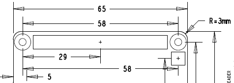
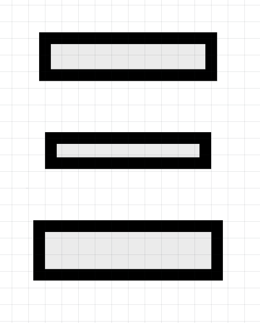
Example below shows a 20mm wide rectangle with a wide Stroke to aid seeing visual difference.
Top uses center of lines (meaning 20mm from Center to Center)
Middle uses Outer edge (meaning 20mm from Outer to Outer)
Bottom uses Inner edge (meaning 20mm from Inner to Inner)
The hole part of this is easy. As noted above, you can’t (AFAIK) drill holes from the board outline svg, you need to (as I did here) drag in a hole from core pcb view, change the radius to 3mm and then position it over the hole in the silkscreen. With the ring thickness set to 0 (as it is here) you will get a 3mm hole with no copper around it. If you want a copper ring, increase the ring thickness as desired (20 thou is the normal for pads) and that will add copper and create the necessary soldermask to leave bare copper. I suspect you are best off with a straight hole no copper though, so that is what I did. The board outline issue is more complex (and I’m less than expert at it). First, the PI3 part is an old 72 dpi part dimensioned in px (which causes scaling issues in Inkscape and sometimes Fritzing). Rescaling it properly indicates your svg matches the rescaled version so I left it alone. However the PI 3 part was overlaying the entire board making selection difficult at times (and probably adding extra silkscreen items we don’t necessarily want.) I fixed this by deleting the connector silkscreen in pcb3.svg (the board outline svg) as it was causing multiple copies of the image (offset by a bit) in the silkscreen. What little documentation there is suggests the path should repeat identically in the board layer and silk screen (I think this will produce silk lines around the board edge), but I did not do that here, just deleted the path for the connector silkscreen outline. Then I overlaid a 40 pin dual row header (which is broken in breadboard but not pcb) and did a “delete minus” on the PI 3 part and moved the connectors so they connected again (so the pads are green not red indicating no connection). That fixes up the connector outline in silkscreen which adjusting the pcb3.svg did not. Note that DRC (routing->Design Rules Check) fails on the between pad connections as it thinks there isn’t sufficient clearance. You may need to check with your board house to see if they can fabricate it (I think it is probably fine but it is worth checking). As the following gerbv output of the generated gerbers:
pcb3.svg with the connector outline removed. It looks to be there, it is just close to invisible, but if you click on the small dot on the line below and right click “save image as” you should get the svg.
Edit: Although it didn’t complain about not being able to render the svg, it also isn’t letting me download it. So here is the svg as an fzp file (so download the .fzp and change the prefix to .svg to get the svg!):