I am designing a board that has no throw hole components and therefore has nothing on the back other than traces, vias amd capacitive touch pads covered by soldermask.
I have made a vector ( svg ) monochrome silk screen design that covers the entire back of the board, this is both for aesthetic and to highlight the capacitive touch pads. This is all good and I’ve imported it into Fritzing and it’s the exact size and everything.
However, when I export the Gerbers for production and view them in any online gerber-viewer, I can see that Fritzing has made holes all over the silkscreen design where ever there is a via. I’m assuming it’s because there are also holes in the soldermask layer where ever there is a via and Fritzing only allows silkscreen over solder mask (?).
Is there a way to prevent this from happening? Either by forcing soldermask over the vias or by editing the silk screen layer manually?
I don’t know the correct answer but I do have a work around for you. Export your gerbers and then delete all the vias and re-export the gerbers again in a different directory. Then use the solder mask and silkscreen layers from the ones you deleted the vias and you will end up with what you want.
1 Like
Thanks sublimeartistry, I hadn’t thought of doing that, this could work but do you know if this will cause any problems with the PCB fabrication and assembly?
Could there be an issue with the silkscreen ink being pushed through the vias and getting close to a pad on the other side, affecting the solder reflow?
I’ve been looking at the silkscreens on the back of Arduinos and they seem to do it without the via being plugged.
My understanding is there can be three treatments for vias; standard open vias, via tenting where the soldermask goes over the hole, and plugged vias where either conductive or non-conductive fill is put into the holes. ( Fritzing doesn’t support the latter two )
Does an unbroken silkscreen design necessitate any measures to be taken in the soldermask layer like tenting or plugging vias?
I honestly don’t know the answer to your question. But I would just make a simple test file and send it to my fab shop and ask if it will be a problem.
Hi Can I just ask one quick silly question? …
Should I be mirroring whatever I want to appear on the back silkscreen layer? I’ve just noticed that when I view the exports all the designs are reversed for the ‘silk_bottom’ layer but not for the ‘silk_top’ layer.
Also, can I make the silkscreen design larger than the board size for ink bleeds or is this generally not accepted by pcb fabricators?
If you are using a Fab shop to make the boards they will only want the Gerber files as they are exported (no changes). If by some chance they want SVG or PDF versions then you will need to ask them what they want (normally the mirroring is for toner transfer and similar methods used at home).
I have never had issues with silkscreen being larger than the board. I think this is because they mill the boards after they are silk-screened.
Also I looked into tenting a little and it looks like all tenting does is put the solder mask and silkscreen over the via and it does not make any other changes in the files so my workaround should be fine (but checking with your fab shop is still advised).
Even exporting the gerbers results in the design I’ve made for the back silkscreen coming out mirrored. I can’t tell if this is because the gerbers are all viewed from above or whether I have to do the mirroring on the svg before setting it in Fritzing.
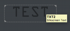
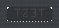
To test this I put logo text object into my Fritzing project on the silkscreen top layer and typed “TEST”… Then I moved it to the silkscreen bottom layer… Doing this mirrors the text.
silkscreen top:
silkscreen bottom:
What’s happening? Do I need to mirror the design I have for the back silkscreen?
In a gerbv you only see the board from the top side so things on the back appear reversed. This is normal and how you want to give them to your shop. So to repeat that differently do not make any changes.
Your pictures look to be from Fritzing and in Fritzing there is a button that says “view from above” or “view from below” which will allow you to look at the board from the bottom at which time it should read correctly.
Cool, all understood now, I just got breifly confused by the Top Layer / Bottom Layer button and the View from Above / View from Below button.
With regards to the silkscreen bleed, I wondered what the standard practice was for creating silkscreens that go to the edge?
Fritzing crops the silkscreen layers on export to match the edge of the board so there isn’t really much for you to do other than place the image/part where you want it.
You can also make the image part of a custom pcb svg. The board file is comprised of a boardoutline group and two silkscreen groups (silkscreen and silkscreen0). You can put whatever you want on the silkscreen layers. Fritzing will also crop these images where they intersect copper pads and vias etc.
lol, nice to hear someone had the same ideas
I actually did make some boards with different soldermasks through two exports
looks fine,
works well if you know what you are doing.
-
for silkscreen design larger than the board size, I think fritzing cut them off while exporting.
or if you mean combining two different size board’s silkscreen for output,
no, I don’t know the answer…
Hi AlanChen. So in order to get my silkscreen design to cover the vias I’ve exported a version of the gerbers where I’ve deleted the vias in question and then copied the silkTop.gbo and the silkBottom.gbo into my main gerber export folder replacing the silkTop.gbo and the silkBottom.gbo that where there.
Will this work as I expect it to? Or do I need to do the same for the maskTop.gts and maskBottom.gbs files?
Sorry for so long unreplying.
if you need your vias covered by mask (the green, or black,white,red,blue,purp,yellow layer that blocks the copper from soldering)
exported the maskTop.gts and maskBottom.gbs with vias deleted for sure,
sometimes the PCB manufacturer can choose the vias to be covered, mostly they follow your gerber
always check your exports with gerber viewer or with a pdf version,
they’ll show if your mask/silkscreens were intended, or not.
wow. this is a question on the fabrication. You don’t do the mirrors for the bottom silkscreen. The engineer in fabrication will handle it. And for the silkscreen covering the vias it is not a problem. Normally the factories will keep a safety distance for the silkscreen texts to the vias. So they would cut some parts of the silkscreen to achieve this.
And the same with the vias. If no soldermask openings design for the vias ,they will be covered(not plug with soldermask) with soldermask. I am a manufacturing engineer and hope it is helpful to you.
Roy