That sounds about right. I’d start with being able to drive the leds. I assume you are driving the leds with the shift registers? If so then you need a variable (probably an int to get 16 positions so you have one position for each of the 10 leds). Next you need to have the software to write that variable out to the shift registers to drive the leds (this is basically the same as the tutorial that writes to the shift registers). Each bit in the variable corresponds to one of the leds being lit, so start by setting one bit in the variable at a time and see that it lights the associated led and turns it off when the bit is cleared. Once that works then you only need to change the bits in the led variable when a button press happens so that the appropriate led turns on and the other led turns off it was on as it will stay on if you don’t turn it off.
Yes I have practiced this and have it in my program with one led. But I’m wanting to add more leds and control them with state changes when certain buttons are pressed
I really tried with shift registers but I just couldn’t manage. Spent days attempting it but didn’t get anywhere. so I got a arduino mega. I really don’t know where to start. I’m sorry to be a pain to all of you guys
Ok that makes things somewhat easier as you now have one I/O port per led. You can do this two ways: copy the same code 20 times and change the I/O pin numbers on each copy or make a subroutine that takes the pin number and a state and call it from the push button code. Basically if you aren’t using the shift registers to multiplex the leds, then if you duplicate the code to drive one led and change the I/O pin numbers to the port for the next led it will drive that led the same way. This is probably where I would start as it will be the easiest (if the least efficient). As an example lets assume you have a red led on port1 and a green led on port2 and the code that drives the leds properly when the push button changes. For the next push button, with the leds on port3 for red and port 4 for green you change port1 from the first code to port3 and port2 from the first code to port4 and the function will now work on a new push button and the two new leds.
I’m not really sure, because a google search on “arduino I/O tutorial” turns up tutorials but they don’t look that relevant. you may be best to post the code that works for a single push button and I can likely tell you how to extend it to more push buttons (which should be just duplicate the code and change the numbers relating to the I/O ports).
I think this would work and is a little more elegant than repeating the code over and over. It is also a good lesson on using arrays and for loops in a simple to understand way. You would have to change the pin numbers and the number of buttons/LEDs to match your setup. You will may also have to change if it is looking for the button to be HIGH or LOW as well as whether the LEDs are on while HIGH or LOW.
//define button pins
int button_0 = 10;
int button_1 = 11;
int button_2 = 12;
int button_3 = 13;
int button_4 = 14;

//define button pin array
int button_array[] {button_0, button_1, button_2, button_3, button_4};

//define LED pins
int led_0 = 3;
int led_1 = 4;
int led_2 = 5;
int led_3 = 6;
int led_4 = 7;

//define led pin array
int led_array[] {led_0, led_1, led_2, led_3, led_4};

void setup() {
for (int i = 0; i < 4; i++) {
pinMode(button_array[i], INPUT);
pinMode(led_array[i], OUTPUT);
}
}

void loop() {
check_buttons();
}

void check_buttons() {
for (int i = 0; i < 4; i++) {
if (digitalRead(button_array[i]) == HIGH) {
digitalWrite(led_array[i], HIGH);
} else {
digitalWrite(led_array[i], LOW);
}
}
}
I have checked and it does compile, beyond that I have not tested this. If it were me I would also only check the button every so often and not every time through the loop (google every_n_milliseconds to learn how).
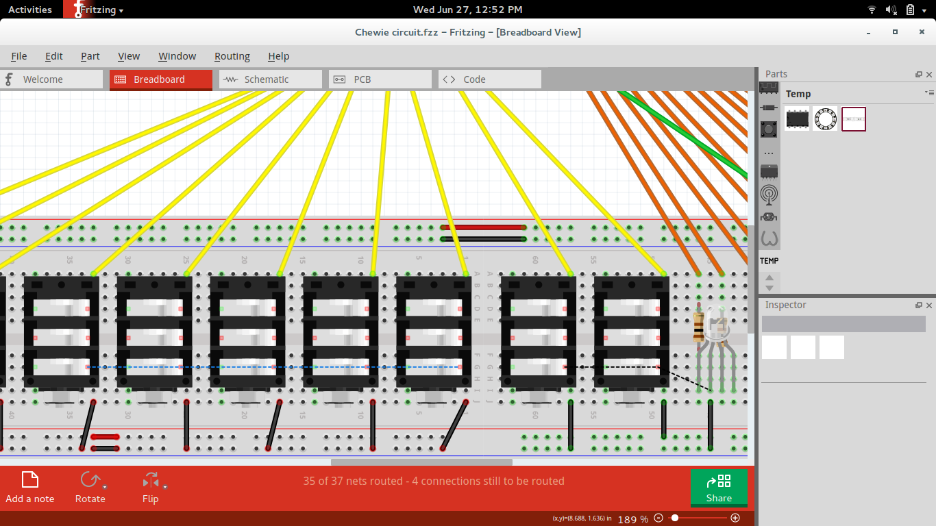
I have finally managed to finish this project, but I am now having some issues with fritzing. I really need to get this on a pcb. But I don’t know how to correctly draw it in fritzing. I have drawn my circuit how I have my physical parts set up on my breadboard. But it is saying I have connections that still need routing. I think it is the jacks. In schematic and pcb views it is a mess. Would someone have a look at my fritzing drawing please? thanks. Here is a image of my actual circuit https://www.dropbox.com/s/z6arjosm06t6cf5/Photo%2026-06-2018%2C%2018%2018%2020.jpg?dl=0 Chewie circuit.fzz (84.8 KB)
In breadboard when you click on the warning at the bottom about connections to be routed it will highlight the connections with little yellow dots. You can also see the dotted lines that connect the pins (ratsnest lines) that indicate the missing connections.
The reason those ratsnest lines exist is because you have made that connection in the schematic view, possibly by mistake. If you do not want those connections then you can right click on the ratsnest lines in breadbaord view and select delete ratsnest line.
As for turning it into a pcb. You now have to figure out the placement of all the components on the PCB. First you may want to figure out the size you want the PCB. I design all my board within a 100mm x 100mm board to be able to order them from Elecrow for $4.90 for 5 pcbs. Once you have your board size figured out and the parts laid out where you think you want them you will start laying out your traces between parts. Make sure you use both sides of the board and do not be surprised if you have to move parts around multiple times to get an effective efficient design. It will take just as long or longer to figure out as the circuit and software has taken already. There are no easy automatic layout tools and almost none but the most expensive EDA programs have good autorouters and even they can take many hours of running and hundreds of thousands of tries to figure what an experienced human can do in less time.
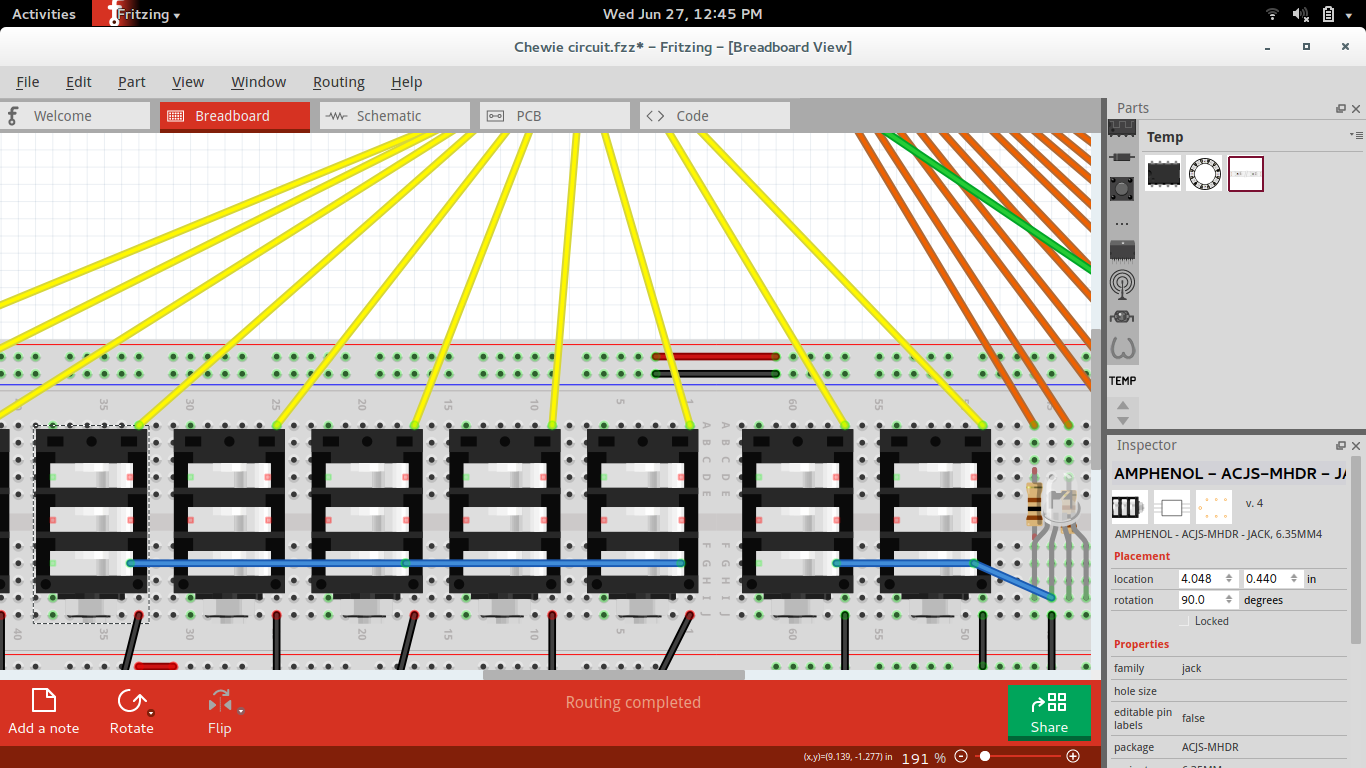
Thank you for your reply, I managed to fix the ratsnest lines like you showed me. The only problem is the schematic view is a real mess and the connections need routing even though I did it in breadboard view. This is where I’m stuck now, I’m not sure as of yet how big my PCB will be. But I just want to figure out my schematic now. How can I fix this mess? Thanks again!
There is no “easy” way to do it. I would start by going to the routing menu while in schematic view and select all traces and then press delete. That should remove any currently routed ratsnests in schematic. Now you would place all the components where you feel like they would best sit (often in the same places as in breadboard view) Then you drag each ratsnests around and when you let go they become wires/traces. You then add bends and route everything in a clear way that is easy to follow. The entire point of the schematic is to allow you to view the circuit and it’s connections to make sure you have everything connected correctly so having it clear is really important.
Be sure to back up your current file before going any further as Fritzing has some bugs that could cause a loss of data.
Also it is not entirely necessary to make the schematic view. If you are 100% confident that the connections are correct in breadboard you can move straight to PCB view. You should always make sure the pins are labelled correctly in PCB view to match your real world parts pin order.
If BB view is your major design, ie you copied a bench design that works, then you have a lot to do.
The 1st thing is you have to get BB perfect - I see mistakes - and you can’t change things in BB view if you have solid connections in SCH view because FZ will alway try to keep them connected in other views.
Go to SCH view and select Routing/Select all Traces, then Edit/Delete
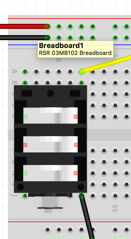
Go back to BB view and look for red dots on the end of wires - these are not connected - and change them until they are connected and green. I see 10 wires links red, jacks with red dots, and a cap not connected.
Once that is perfect go to SCH and use the ratsnest to connect stuff - you can click on a part pin and what ever is connected to it will turn yellow to find a better connection.
Go to PCB and spread out parts, position them roughly on an oversize PCB - you can resize it latter -, move stuff into a corner until it looks good, and then join traces trusting the ratsnest like you did in SCH view.
If SCH is the major view you can work it out from the above.
Thank you for your reply, I never noticed the red dots on the breadboard view. I have fixed them. I also deleted the ratsnest lines in schematic view. But I have just realised I used the wrong 3.5mm audio jacks. I need the 4 leg version. But unable to find one in fritzing. I did find one but it wouldn’t fit across the board. Where can I find one of these? thanks Chewie circuit.fzz (80.1 KB)
Can you provide a link to the correct datasheet for the component. Once we see the footprint we may be able to point you in the right direction or possibly create the part for you.
If you look on page 116 of that datasheet you will see the footprints for each part. It shows that they use the 6 pin stereo footprint even when using a mono 4 pin part. Unfortunately the part you had had slightly different pin spacings. I have edited that part and created a new version called ACJM-MH for you and I think I got the spacing correct. To be sure I would create a new sketch, import the part, place it on the PCB and then print the PDF/SVG via the Export for production button at the bottom. Then you can place the part you have on the print out and make sure it is the correct spacing. The difference between some of the variants is on 0.1mm.
Also after modifying that part I would say the orginal part you used would not work with any real jack as the spacing of the pins was a combination of the one you wanted and the one it was labelled as.
As I said the datasheet specified the 6 pin layout for the 4 pin part. If the extra legs cause you routing issues then it would be no problem to make a mono only part but it would be non-standard layout. The good part of using the 6 pin layout is you can use stereo jack if they are easier to get or cheaper and it would still work with the mono male connector as if it was the mono jack.
Sorry! I completely ignored what you had previously said. I will try with the one you have made for me and hopefully it won’t cause any routing problems. Thank you for your help I appreciate it!
I’ve had a go at using the part you made. I can’t seem to get the right hand side pins to fit into the breadboard holes. Can’t line any of the wires up, or am I doing something wrong?
