the power board and the ESP board will connect to each other via pins on the top and bottom of the boards (sandwich). the third board is a relay board that will be located on the opposite side of the box where all components will be installed.
the designs are a combination of research and personal knowledge.
a second or third set of eyes is greatly appreciated.
I’d suggest that properly routed schematic views would be a good start to the review process. The schematic view in the first 2 downloads is still the rats nest and basically unreadable. Having a proper schematic I could look over the PCB and see if it looked right. I assume you have already done a design rules check in the PCB view (Routing->Design Rules Check)?
thanks all for the help and guidance. this is my first time using the fritzing to produce my designs. i have been using 4x6 boards and soldering wires from point to point.
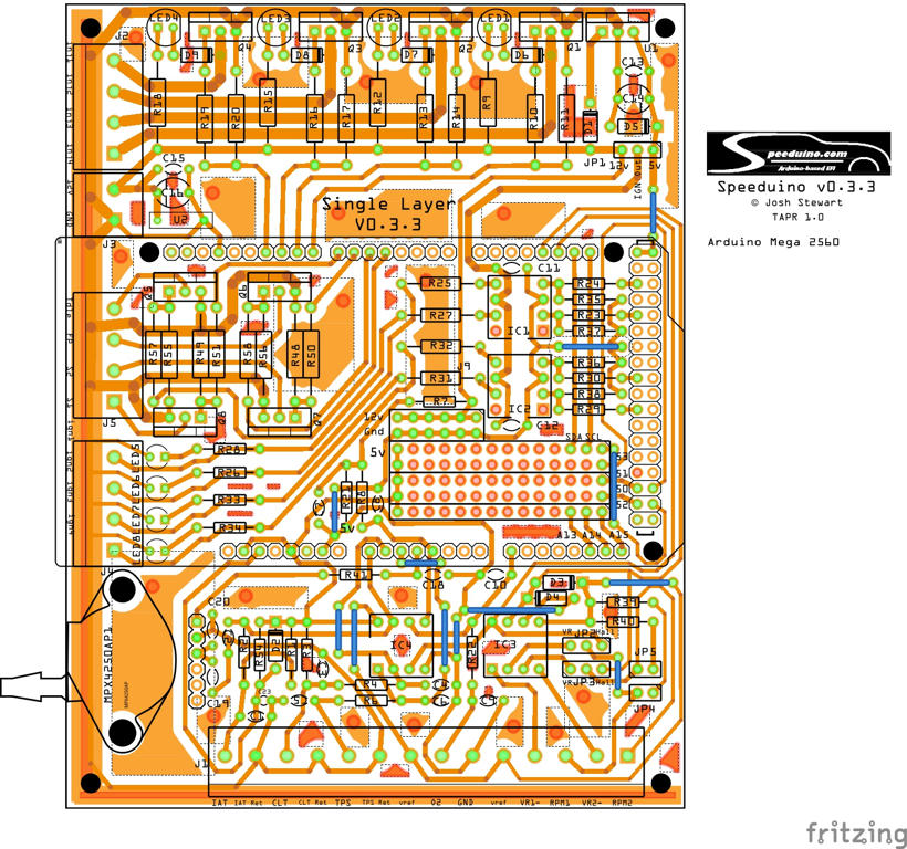
so i have modified the designs according to everyones suggestions and guidance. take a look and let me know what you all think…
i did run the DRC on the boards… unfortunately i had to correct the controller board AFTER i posted my modified boards. just ignore the three items listed in the DRC, they are fixed.
changed the tracks. i am not using the imperial system but instead using the metric system since i am in Germany and its easier to use for other devices that have MM vice IN
good catch on the JP2 and JP7. i did not and changed the design. as for the silkscreen items, they are written in that direction to identify the voltage on each of the pins. the other items were changed to be oriented in the same direction.
Thankfully I didn’t have to design that - I’m not that smart -, all I had to do was shuffle parts around for a couple of weeks until I converted it from double sided to single sided. Oddly enough my single ended up smaller than the original double. That’s only V1, my final one with added circuits and stuff is even more complicated.
This is what I meant about stretching FZ to the limit, because when I tried to ground plane it I couldn’t get some of the contacts thermal isolators to stick. Some stuck, some just wouldn’t, so I gave up on ground plane.
Although it has an as bad or perhaps worse learning curve, you may actually need kicad I came this way from there because I typically don’t make boards and the breadboard view is much better for one of perfboard documentation but they are aiming at the serious pcb marketplace which may be a better fit for you.
I know about KiCad, and still use GerbView, I just don’t like it. KiCad is a bunch of separate programs that don’t talk to each other in one wrapper. In KiCad you do the SCH, export the part file, define the parts, and then import it into the PCB view. Fritzing has all views connected instantaneously, and has an added Breadboard view, and the price you pay for this convenience is that parts are a bit harder to make. KiCad looks like a DOS era program because it so crude, where as FZ looks like a modern Windows program. KiCad has an internal parts drawing program, which is a lot quicker than the svg route we have to do, but everything looks simple and basic. It basically doesn’t have the eyecandy BB view parts that FZ has - which are as addictive as real candy -, that is a winner with beginners.
i downloaded the program and started to read through the docs. i like fritzing because i can get the boards produced directly from the APP. so within KiCad, how would you get the boards produced?
Sorry, my mistake, I was referring to Old_Grey developing his new expanded Speeduino board. KiCad is a little more complicated than FZ. Before going to KiCad, DipTrace, Eagle, or something else I would strongly recommend sticking with FZ. For the board you want to make, FZ is the place to start, then when you get FZ down to a science, picking up KiCad will be much easier to understand. Fritzing, KiCad, Eagle… all have their place… FZ was designed as an educational tool to learn the relationship between your breadboard, schematic, and PCB. Personally, I use FZ, but I don’t make any large complicated boards either. I like FZ for the same reasons everyone else does…

