Part request to apa102-2020

Here is a start. I think it would make a workable PCB at the moment but it does need a new Schematic and Breadboard because it has two pads for Vcc and two for GND in the middle which is two more than the WS2812 that I started with.

Part removed. See Part request to apa102-2020

For my contribution to this project, said new bb and schematic (which required renumbering the pcb pins as well):

edit due to an apparent error in the data sheet this part is incorrect and has been deleted until we can make a proper one.

as always, print out a copy and check the footprint matches the device you actually have before committing to boards …

Peter

Good work Peter. Hopefully it will work for @AlanChen .

@Old_Grey
@sublimeartistry
@vanepp

thanks you all for the help,
can’t believe you guys can draw with this so fast :fearful:

comparing my “footprint made with pure pads” to yours
there’s a bit different, but the actual part is more symmetric and look like yours.
I guess it’d work, and can’t wait for :slight_smile:

just did a try with 100 part copies, and they moved smoothly :smile:

btw, drawing wires,part with such dense pads can easily link to neighbor pads in Fritzing, is there any way to change
the default trace width?

Yes, just click on the trace, and in Inspector type any thickness trace up to 128"

Just remember some PCB manufactures don’t do less than 0.006"

Remember to print out the PCB and check that it is 100% right, because you don’t what to have to do a second one. Check that the footprint is bigger than the part so you can solder it from the side.

Default trace width, No. Unfortunately that is not something they have implemented yet. Although it is something that has been requested Global track thickness setting - #2 by sublimeartistry But as you are most likely aware Fritzing has slowed down on development so it may not be something that gets implemented unless one of us figure out how.

I do see that my pad is a little different then yours. My pads are the exact dimensions given in the datasheet for the solder pads.

Also one last thing. You may notice the silkscreen I added to the footprint overlaps the pads but on export Fritzing crops them to be between the pads.

1 Like

Oh default. opps.

You can Routing/Select All Traces and change them all in 1 hit, it’s just you would have to make all the small traces first and change them in a group and then make the others.

You can CTRL-click select all the traces one by one, and again group change them in Insp.

While parts creation has a steep learning curve, once you get over that parts are reasonably easy to make.

If you are planning a project with a lot of these, you need to be aware of their power issue (which you may already be). The internal oscillator in each chip is asynchronous so unlike sync multiplexer schemes the power does not average out. That means it is possible (and in fact likely, at at least some times) that all the chips will be drawing full power at the same time which (if you don’t size the power supply appropriately) will cause seemingly random failures as the power drops and the chips reset. You either need a single power supply (and distribution system) capable of powering all the leds at full current at once or a series of smaller power supplies that can power a single or a couple of chips at full load (this can make distribution easier in terms of resistive loss in the power wiring.)

Peter

1 Like

thanks for your awareness, I know, and power was planned to be separated with N-channel mos
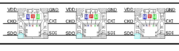
Apa102 were widely used in POV projects, mostly sold in 5050 package LED strips

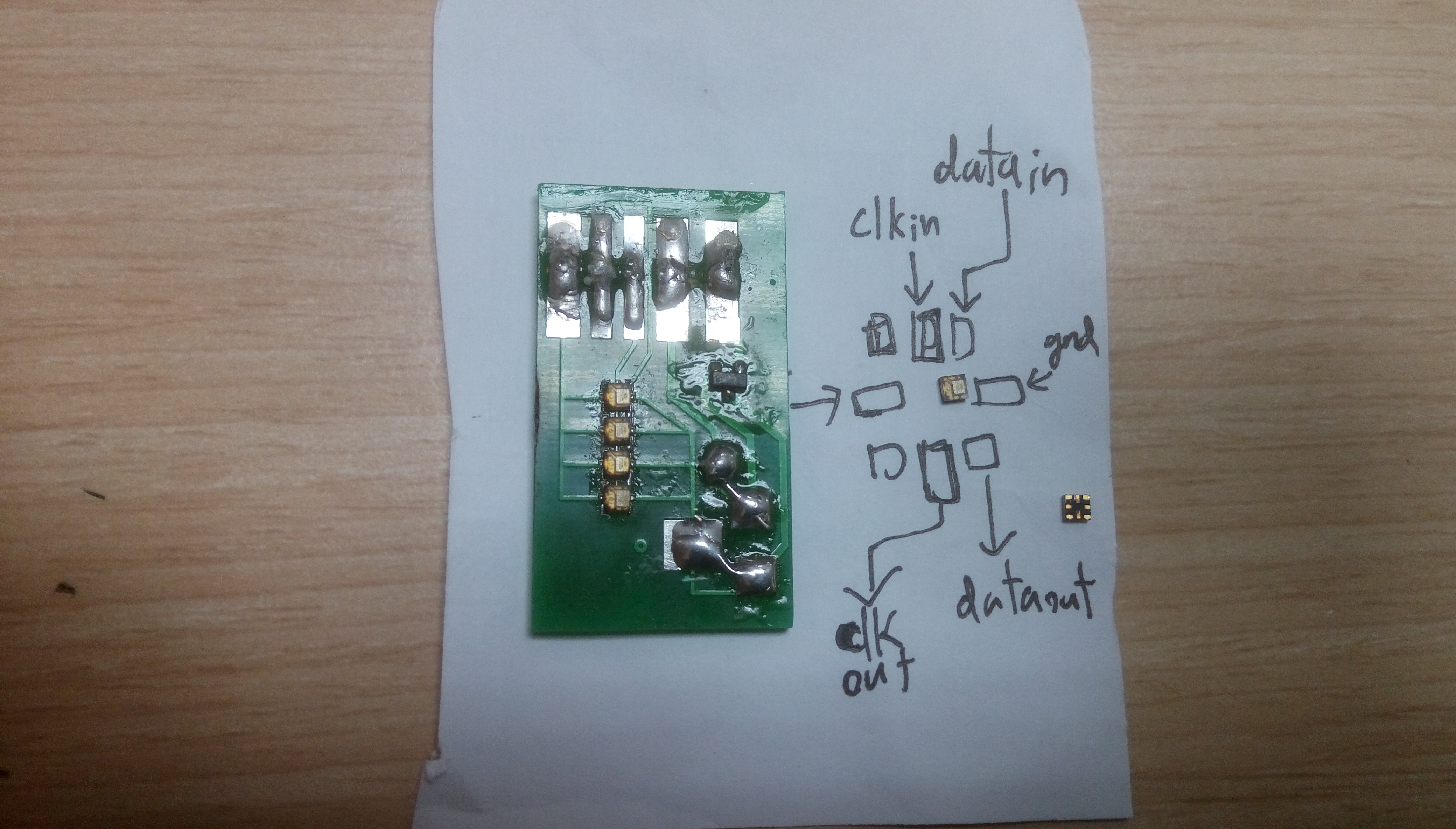
and this is not my first POV, likely 5th if i count. :slight_smile: 2020 is not friendly for hand solder,
got a hot air gun&paste and already experienced with success air-soldering
I pick 2020 because it’s small, can do dense POV, and its simple integrated driver

with a 18650 Lithium battery I got my POV with 72 apa102 -5050LEDs working well
I hope 100s of them, in 2020, work well too,

If not, I’ll parallel a second battery, :wink:

oh about part creation,
maybe I just can’t hold inkscape crashing all the time,
I can draw my own board shape(and inkscape mess it up often)
but part’s kinda much for me yet

breaking up to pads works well with easy/small parts to me,
most likely due to I use strange parts, such like some switchs(like those in hand-flashlights) , they dont have pins or leads, not a PTH/SMD part in general.
and needs custom designed pads for soldering, depends on how I’m using them. :confused:

@Old_Grey sure, select all trace and change
are there group and layer like those features in PS/Sketchup/CAD in Fritzing?
if not, its still kinda better for me to set traces for each in this case,
I got my power lines as wide as possible, and SPI lines to 8-12 mils as they’re under the part, short and don’t need to be wide.

thanks for all :sunny:

Which OS are you on? For me on Win7 Ink rarely crashes (xml editor screwups are the most common cause there, it doesn’t like some types of group indenting) but a crash is pretty rare. When you say Inkscape messes the shape up, does that mean the scale gets wrong (i.e. its larger than it should be in Fritzing)? That can be caused by not having the document length and width set to units (it defaults to px which can cause scaling problems).

Peter

I’ll start by saying I love LEDs. https://theledroom.wordpress.com/ which is one of the reasons I decided to help with this footprint. I have a large collection of Individually Addressable LEDs but never enough as it turns out. I have a project that needs a few thousand I.A. LEDs and the smaller the better so why not try out these 2020 ones. I started to design a board with the part from Peter above but found that the recommended footprint (the one I made from the data sheet) did not work well when trying to design a compact layout. My solution was to modify the footprint to allow the two GND pads to be connected under the chip (top left and bottom middle).

This makes some of the pads very small (although still larger than the pads on the LED).

Image and part removed. See Part request to apa102-2020

Thanks to @Sublimeartistry ;s good eyes I have found a bunch of errors which I think make this part currently incorrect. I’m working at correcting them and will post a corrected part a bit later. Hopefully you haven’t gotten too far with the current part …

Peter

Don’t you hate that.

I think if you make it the same family you can do a direct swap out by selecting in Insp.

Ok, I think the original part is indeed incorrect, for reasons I don’t understand the pcb seems to be rotating on import, and without a pin1 marker it was difficult to see the original part is flipped and won’t line up properly with a real chip (the pins would be reversed, connector0 / pin1 on the right instead of the left as it should be). For this corrected (I hope!) part I grabbed @Sublimeartistry 's latest footprint, added a silkscreen group (it was just the rectangle) and added two lines to mark pin 1 (although there doesn’t appear to be any way to tell on the chip that I can see in the data sheet) and changed the pin numbering to match that on the data sheet (with the extra ground as connector6 / pin7 and the extra VCC as connector7 / Pin 8 as they aren’t numbered on the data sheet). In schematic I changed the pin numbering to match the new scheme (which puts the pin numbers out of order, but matches the chip and bb layout) and corrected the names to CLKI (instead of 1) and CLKO (instead of 0) as they should be. On bb I rotated the image by 90 degrees to align it properly and moved the input pins to the left and output pins to the right as is standard. Again the pin numbers are out of order, but they match the physical layout of the chip which I think is the best choice. I changed the variant to 2 in the fpz file and corrected the label on one of the grounds (which was set to VCC), but I don’t think a straight replacement is likely to work as the pin numbers have changed. This one is a new part and should coexist with the others. If anybody knows how to stop pcb from rotating I’d like to hear it (because is annoying having to rotate it to the correct orientation).

edit: there looks to be an error in the data sheet and this part is incorrect. Deleted til we can make
a proper part.

Peter

did I started a crazy topic? :lol

not yet too far yet, 40copys chained

I’ll upload my working prototype to show the directions of the part.
it’s kinda hard to tell which directions’ in/out from the front side (and back) of the chip

but yeah, it works anyway

also, there seems to be different 2020 packages on the market, with different footprint
i haven’t tried or seen any of them besides mine,

Here is my working prototype. With my “pads part”
Footprint, one can find the board from the APA-102-2020 - the ultimate smd addressable led.
The package is distinguishable from top,but can’t from bottom
There’s IC implanted in right side of the chip,
And leds in the left.

The density is 4LED/cm
Hopefully could be as dense as 5/cm, with specialized footprints
But there are power pins on the side of the package so I’m afraid of shortage

edit: from observations, the Din/Cin and Dout/Cout were inverted in your footprints,
just need to switch label Din<->Dout, and Cin<->Cout

yes,yes
using W7,too , sometimes W10
not sure if Chinese Big5 OS language is possibly a problem?
much crashes on xml editting,

and yes, the board designed, shrink in height direction but not width.
so I need a few try, and even txt-edit the .svg for fitting.
thanks, will try to look into default unit next time.

@sublimeartistry
my next wish is that Fritzing can do 4-layer or more layer boards,
so that power line and gnd can easily hidden,
but 2020 for me, there is still plenty of room for power lines on board.

@vanepp

Actually every single part we have made so far is wrong. I wish they had a good datasheet available.
If we look at this picture from the datasheet we can see that when viewed from above the top left is vcc and the top right is gnd which is opposite of all the versions we have made so far (and opposite of the diagram next to the pad layout in the datasheet). As well as the previously mentioned In and Outs being on the wrong sides.

Basically so far we have only actually got 2 of 8 pins correct :joy:
I am going to delete all of my above uploads as to prevent anyone from trying to use them in the future.

1 Like

Yep I had just come to the same conclusion, based on the working board the data sheet appears to be wrong, and thus so are all the parts. I agree we should delete them all while we regroup :slight_smile: .

edit: I think your latest footprint should be fine (as our understanding of the pin numbers seems to be the error) so I’ll start from that and the original working footprint and try again …

Peter

That is possible, but it may also be a bad setting in preferences because I use xml edit a lot and other than the group issue (which is mostly my own fault) haven’t had any crashes. There are so many settings available its possible something is set wrong. I have found that if you hit a wrong key Inkscape will happily update preferences and remain screwed up. I generally keep a copy of the

C:\Users\Owner\AppData\Roaming\inkscape\preferences.xml

around and replace it when I screw something up. That may be worth trying (if you can get a copy from a default install somewhere).

Peter