What are the rules regarding asking some someone to designing boards for me, paid work?
Thanks
Brian
What are the rules regarding asking some someone to designing boards for me, paid work?
Thanks
Brian
Just supply an outline as to how complex it is, and someone might be interested.
Hi All
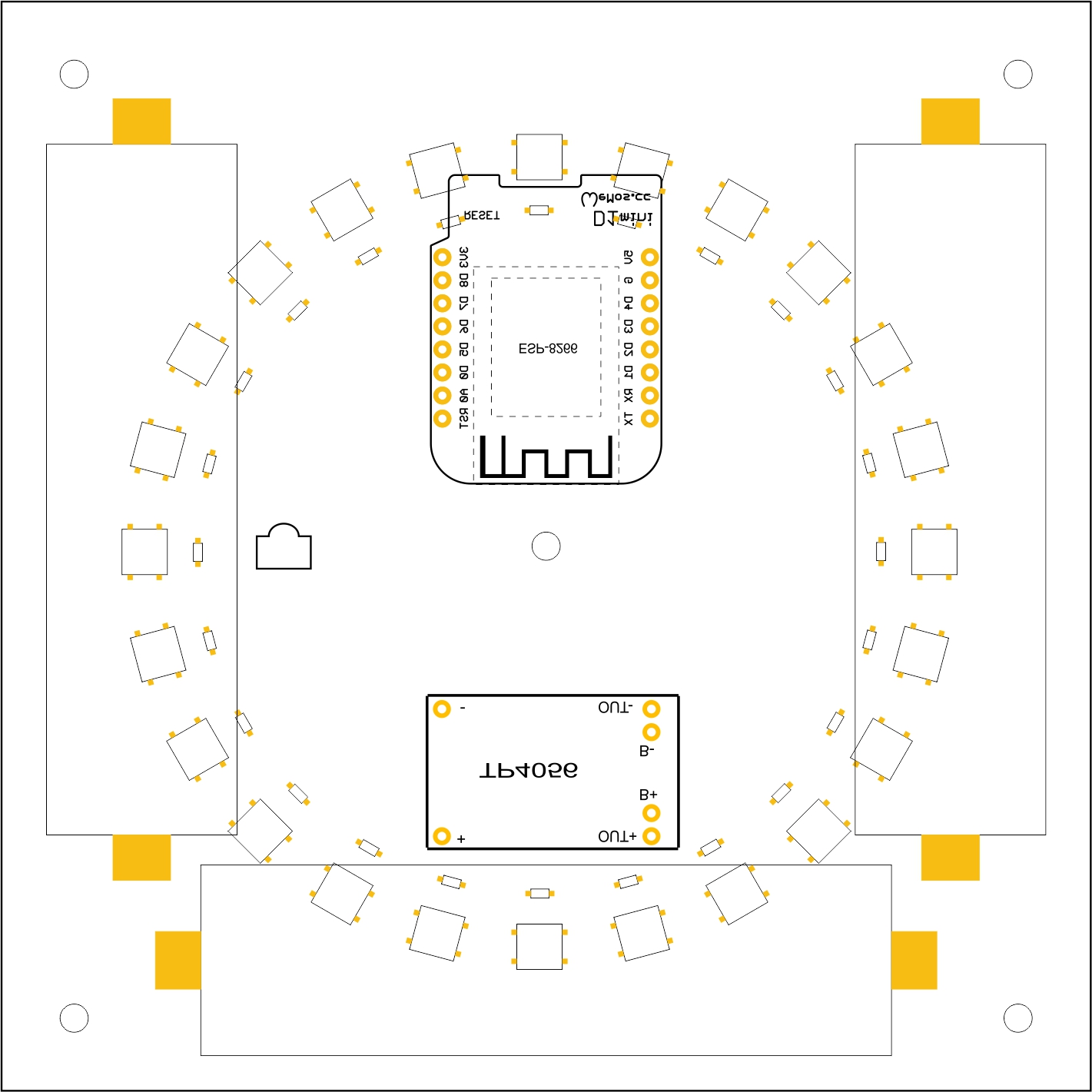
I’m working on a project using 24 x WS2812 LEDs in a circle, ESP8266 D1 Mini, TP4056 and 3 single 18650 battery holders. I have never done any board design so I’m a little out of my comfort zone. The main issues I have how to lay out the WS2812, the pad sizes, track size etc, there is also a surface mount capacitor by each LED
After posting my message last night I’ve had a think, I’m still developing this project and could end up going back and forth with design changes. So going to take a different (and possible better) approach, and for some with the correct knowledge this is probably something they could do in there sleep :).
Instead of designing the whole board, I will need the components designed to match my requirements, I will then do the layout myself, and the same person that did the component design to check my work.
As I say this is paid work, if you are interested please let me know.
** Design brief **
I need someone with good design skills and understanding of PCB design and fritzing to design 2 components, a 18650 battery holder based on the specs of the ones I will be using, and a ring of 24 WS2811b LED.
18650 battery holder
I’m looking at a surface mount 18650 holder, using surface mount means not having to have through holds. This helps with the design layout for the overall project.
I’m looking at purchasing these:
LINK
I would need this designed as a Fritzing component
24 WS2811b
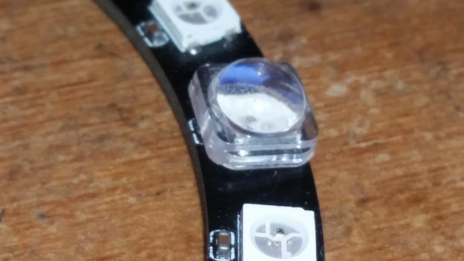
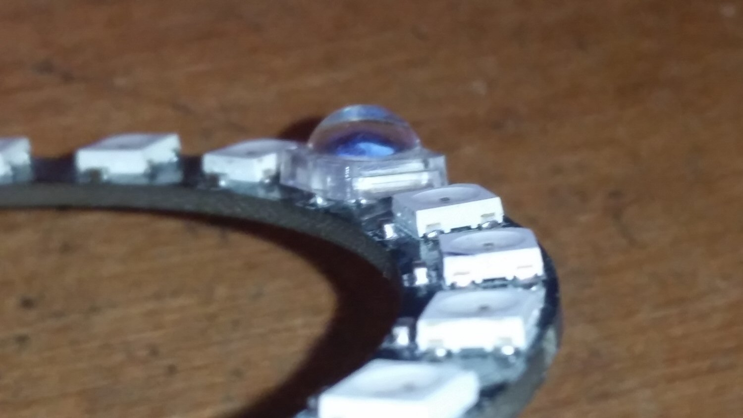
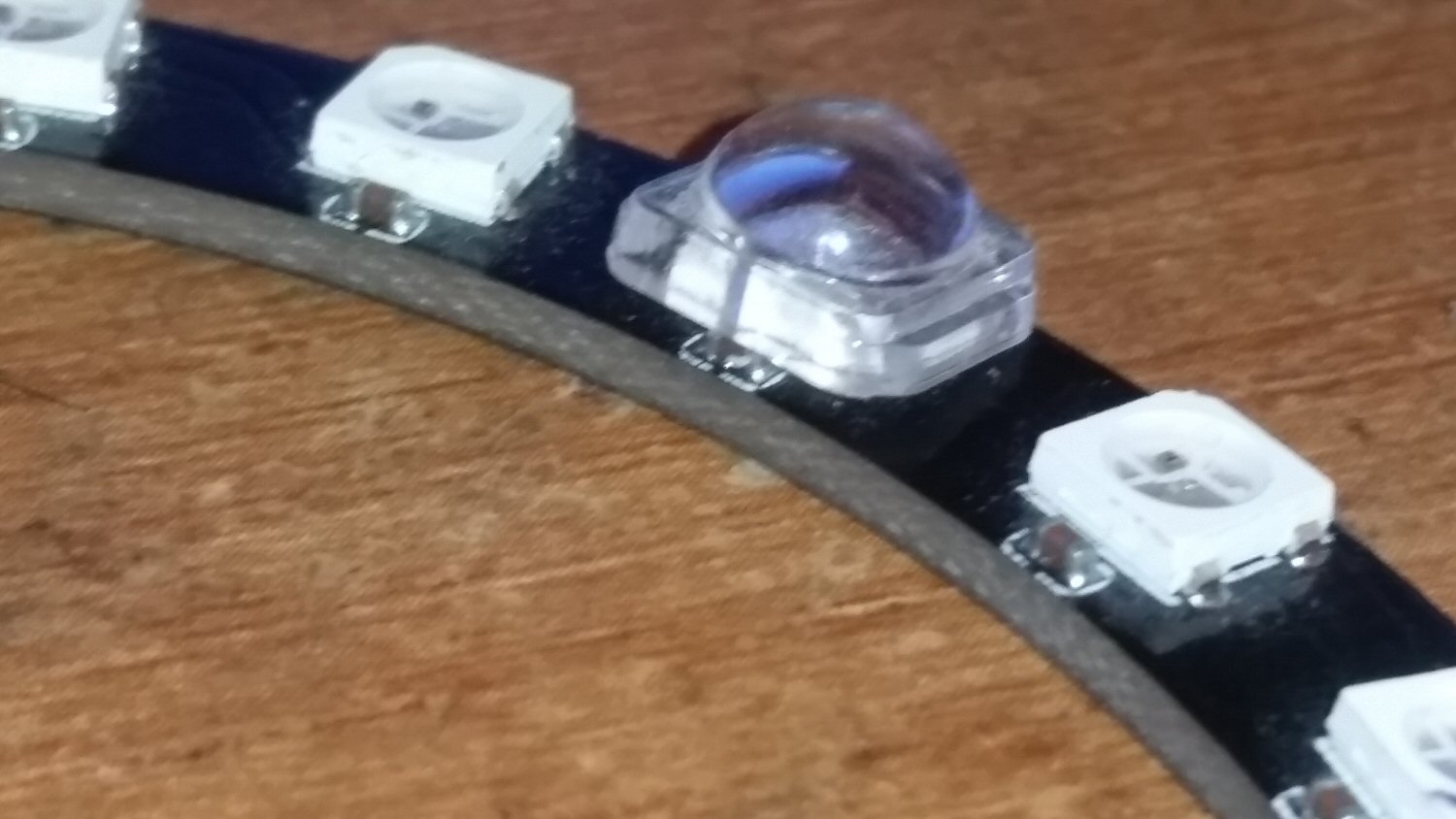
This is the one that is outside of my skill set, a Fritzing component that comprises of 24 WS2811b LEDs. This will allow me to drop this onto my board design as required and place the tracks. As said above, there is a capacitor for each LED, this needs to b set on the inside of the LED and far enough away for a lens to be placed over the ring. The placement of the lens is one of the main reason I can’t use an off the shelve rings as the capacitor stop the lens being fitted.
You will need to know, understand and have the knowledge on what capacitor is needed in order to design the component .
Here is a mockup of where I am heading.
Thanks
Brian
The 18650 battery box is trivial I’ve already done a couple of them through hole, so an SMD version is minor. Do you have a LED in mind (the WS2811b is the controller chip not a led)? Adufruit already has Fritzing parts for their neopixel LEDs and I did a part on a fine pitch 2020 (as opposed to the more normal 5050) led some time back, so there are parts around that can be adapted easily, but we need the package of the exact LED you want to use. Here is a part for the battery holder:
18650 battery holder-SMD.fzpz (11.9 KB)
Peter
Hi Peter
Firstly, thanks for the battery holder, that’s a beer I owe you already sir !!
With regards to the LED, yes sorry I should have stated it’s the 5050 all in one package, that contains the chip.
https://cdn-shop.adafruit.com/datasheets/WS2812B.pdf
As I say I can’t use off the shelve rings as when I try to put lens on they do sit on the capacitor (see photos below), plus I’m making a custom PCB, I then will be getting a company (probable china based) to manufacture the PCB and populate them with the LEDs and capacitor, then all I need to do it load the D1 Mini and TP4056.
What I am looking for is a component created where all the LEDs have the tracks already linked together supplying Pos and Neg, Dat in and Out, linking to the capacitor as required, then a point where I connect the tracks to. I can then drop this onto my board and connect the power and data as required, these connections will need to be VIA holes.
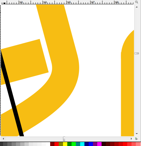
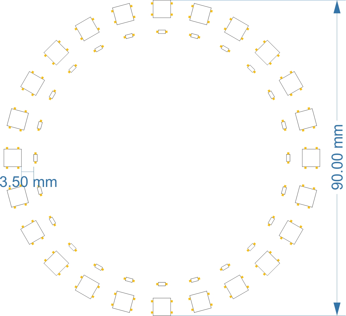
Below is a better diagram of the sizes, from edge to edge of the LEDs has to be 90mm, and the capacitor has to be 3.5mm away from the inside edge of the LEDs allowing room for the lens to be placed on.
Brian
The LED is already in core parts, just type 5050 led in to the parts bin search and the first one that comes up looks to be the correct footprint… I assume the caps will be 802 type case so they are standard too. All you need to do is lay them out in the desired radius in pcb view and hook the traces together. The most exciting part is probably getting the angles in the circle correct. Adafruit has led rings, I assume they don’t have the size you need? I don’t immediately know how to get a circle in pcb view. I’d probably import an SVG of the cricle of the appropriate size, but I expect there is a standard way to create a circle of a given radius, I just don’t know what that is. After that this is pretty easy just hook the pins together with traces and leave one section of the ring with the input to the first led and nothing on the outputs of the last led.
Edit:
30 seconds of thought produced this:
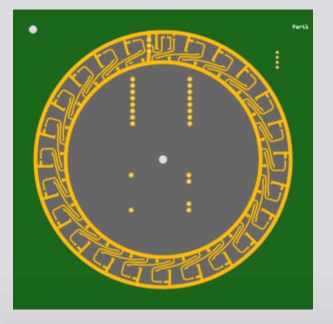
led-circle-sketch.fzz (16.7 KB)
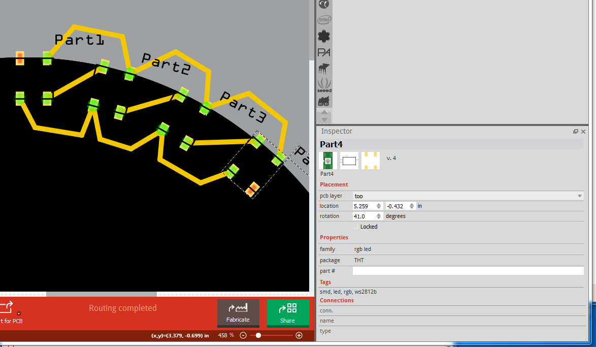
The 90m circle is a hole set to 90mm diameter. I expanded the size of the board area and added in three copies of the battery (I didn’t do the capacitors but I expoect they are across power (i.e vdd to vcc) and are thus trivial to dd. The only somewhat exciting part is placing the leds. For that you need to do this:
Drag the led in to the drawing (or more usually duplicate an existing one, either works), drag it to the new position (part3 in this case) then use the Inspector window on the right to modify the rotation angle (I just held down the arrow beside the rotation value til it looked right, then drag in the connections it needs and place them. You would likely need to make thicker traces and/or a ground fill because these things sometimes draw large currents, but its all pretty easy to do yourself. You do need to be careful of the 18650s. You should add a protection board to them, as if shorted they will explode (and the protection boards typically take care of charging as well)
PS you need to delete the hole when you are finished laying out the leds as the hole will destroy all the copper if left in.
Peter
Hi Peter
You would think this was easy to do, its taken me hours to create a graphic that work (I hope) that’s on a single layer. Having vdd to vcc rails and being able to fit the caps and making it a perfect circle isn’t that easy, which is why I wanted to paid someone to make it.
Firstly the circle has to be perfect, second the caps have be far enough away allow the lens to be fitted and 3rd I want it a single component, this way there is not way I could accidentally move something as it moves as one.
Second, I have very limited knowledge on PCB design, you say the caps are probably 802, unfortunately I don’t know what and 802 is, but I need to know exactly.
I’ve been working on the below graphic, the what I now need what the capacitor is so I then know how to set up the pads, then I have the fun of trying to get is as a part

Regards
Brian
If you pick the value of the capacitor you want to use, its data sheet should tell you what case it is (602 and 804 are common ones). With that in hand select a ceramic cap from core parts and you cab get either a 602 or 804 smd footprint to copy. The next bit of excitement (which I’m not likely to be much help with) is setting up the circular board outline to get the circular edge and the hole in the middle. There have been posts in the forum about making odd board shapes and perhaps one of the folks that have done it will chime in. You also need to make a bit more clearance (about 10 to 20 thou is best, although the board houses can get down to about 8 thou I think) between any two traces. This one as an example needs to move right a bit (centered between the two traces would be best). It looks pretty good though.
I expect you will want to add holes for the lens to mount it beside the leds somewhere too . One other note on the LEDs: don’t believe the common (on the suppier’s web sites) advise that you can get a way with a fraction of the maximum current draw because of multiplexing. That only applies to syncroness multiplexing and the WS2812 is asyncroness and will sometimes draw full current for all leds at once, so you need to design you power source to be able to handle that. The clocks internal to the WS2812 are set by a rc oscillator and are not syncronized between chips.
Peter
After many hours i have got the right spacing for everything, however ive hit a problem, its has to do with the mask but i don’t know what info i need to know to fix it. What should happen is i end up with exposed pads and the tracks have a mask on them, what ive not is a large exposed part with all the tracks exposed.
Any idea on how to set the tacks and the pads?
Thanks
Brian
The simple answer is no  , (and hopefully someone that does know will chip in here!), but I suspect you need a mask layer in the svg although I’m not aware of a part that has one to use as an example. For usual parts Fritzing does this for itself exposing all the copper in the part on the assumption (incorrect in this case) that it all wants to be solderable. I assume it is possible to do the same in one of the optional layers (although I may also be wrong ). If you upload the svg (you may need to rename it to fzp as the forum often won’t render complex svgs) to upload it, I’ll have a look and see if I can find a solution if no one else pipes up.
Peter
Thanks Peter
Ill will also make a new post in the main forum with the correct subject on the problem
BrainLED Ring MKII.fzp (45.4 KB)
That would probably be a good bet. I had a look at previous articles, and there has been some discussion about this but no clear answers that I saw. The gerber code apparently does the solder mask stuff, and there may not be a layer that will do it, but I’m well out of my area of expertise here. I’ll look over the svg and see what I can come up with.
Peter
I think i have read every post on this as well, nobody seems to know the answer. This may have just put on stop on my using Fritzing which i s shame as i like it and im starting to get my head round it
Brian
I think the answer is likely to generate the mask you need as a gerber layer and then substitute it after gerber generation which will generally be a pain I expect. The only posts I see are the other direction: using invisible copper to block solder mask which is the opposite of what you need to do. It looks like the gerber code automatically generates solder mask on anything that isn’t copper in a part but everything in your svg is considered a part and thus doesn’t get masked. I’ll keep thinking about a way to do it, but unless someone else has a clever idea I don’t think its possible.
Peter