Hi All.
I would really like to use Friting for my current project.
I would like to use the HC-05 bluetooth module, but not on a carrier board.
All the parts I have found are on the board.
Does anyone have this part they have made in the past?
Hi All.
I would really like to use Friting for my current project.
I would like to use the HC-05 bluetooth module, but not on a carrier board.
All the parts I have found are on the board.
Does anyone have this part they have made in the past?
So you want just the green bit with the half holes. That’s going to be a bit of work because it’s all 3 views.
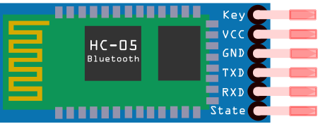

Yes, that’s exactly it. I want to use it on my board directly.
It has been done before, but the person who did it is not responding on the forum I found it on.

Is there any .fzz or .fzpz files?
EDIT
It’s got a different footprint than I thought, much easier

Sadly not, that’s what I was trying to get from him.
And yes, i should have explained clearer.
I just need square pads that I can solder the bluetooth module too.
Much like an esp-12E
If you search Bluetooth in FZ is the BTM182 or the Bluetooth SMD module the same.
Thank you.
I’ve had a look and they are similar but not the same.
The number of pins don’t quite match.
But should give me a starting point
It seems that those are a touch out because it’s supposed to be 1.5mm pitch.
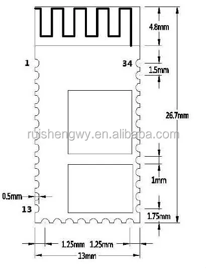
I just came to the same conclusion.
What do you think is the easiest way to get one to fit my footprint ?
The fritzing bluetooth smd part appears to be 1.2mm pitch so you need to increase the footprint to 1.5mm using Inkscape and then create a new part. The official footprint appears to be here:
https://www.itead.cc/wiki/Serial_Port_Bluetooth_Module_(Master/Slave)_:_HC-05#Hardware
If you are unfamiliar with Inkscape I can arrange to do it easily enough.
Peter
I do not believe that other person actually made a part. If you look at the picture you will see little lock icons on every single pad. This implies they used single SMD headers for each and every pad.
If you only need PCB view it would be relatively easy to make a part starting from a generic IC and just change the PCB view.
One more thing. If I were making the PCB layout I would only have the pads I needed (tx, rx, led1, led2, key, 3.3v) etc. This way you can route traces where the other pads would be since the extra pads are of little use in most cases.
Hi Peter.
If you have a minute could you alter/create the part for me please.
I am a software engineer and this is my first dabble into hardware for one of my personal projects.
I don’t min the learning curve of PCB design but making the parts is a bit too far at the moment.
That’s an interesting though.
I’ll see what @vanepp comes back with.
I plan to take the pads I need through to the other side of the board anyway for now so am fine to have all the pads.
I’m inclined to do all the pads so the part is general purpose if someone in future needs all the pads.
Peter
That’s perfect, Thank you.
I believe the part will suit both the HC-05 and HC-06.
The pinouts differ, but the functionality is the same.
Try this one, I think it should be right. You do need to verify the footprint against a real part before ordering boards though.
Bluetooth HC05 SMD.fzpz (11.9 KB)
Peter
Thanks.
I’ll have a play and report back 
Good, changes to the part are easy, boards made from a bad part not so easy . One thing I notice is the pads are on both layes. I tried only using copper1 (as the part file format suggests) but then it is only on the top of the board, you can’t put it on the bottom. There may be a trick to this that I don’t know yet as I rarely use smd (or boards for that matter).
Peter
I just sent @Vanepp a PM with a working SMD part I made but I couldn’t remember what changes I made to make it work so I will let you use your XML foo to figure out the differences.
